Abstract: This ar
ticle describes an appl
ications circuit f
or the MAX4455 Arbitrary Graphics On-Screen Display Video Generator to reduce the effects of fini
te switching time on the insertion of graphics onto a video signal.
This application note describes a circuit modification to the MAX4455 EV board that will improve the pe
rformance of the MAX4455/MAX4358 chip set by reducing on-screen display (O
SD) artifacts caused by finite switch time effects. This modification
can be included in any
similar MAX4455/MAX4358 application circuit yielding the same performance improvements.
The MAX4455 is an 8-channel arbitrary graphics OSD generator and the MAX4358 is a 32 x 16 c
rosspoint switch with integrated fast MUX for OSD insertion.
Explanation of Finite Switch Time Effect
In the MAX4455 there are two outputs involved in the generation of the OSD graphics: the fi
rst output, the OSDFILL, is the
analog representation of the video fill signal, and the second output, the OSDKEY, is a digital signal that controls the turn on and turn off of the fast MUX switch. They are synchronized to within a nanosecond or so at the output of the MAX4455.
Due to the finite switching time of the fast MUX in the MAX4358, the OSDFILL signal emerges slightly delayed from the OSDKEY signal. This results in a slightly delayed OSDFILL graphic with a tr
ailing bl
ack level (0 IRE) equal in width to the switch delay time (as shown in Figure 1). This effect may be objectionable in applications that display all white characters, due to the high contrast between the white character and the trailing black edge. This is even more obvious on a light background due to the light dark light pattern.
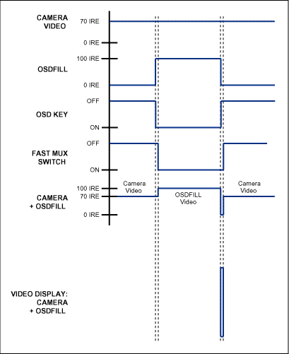
Figure 1. Finite switch time effect.
Circuit Solution
With the circuit modification shown in Figure 2, the trailing black level will be replaced with a trailing white level. If this white level equals the OSDFILL level then the trail effectively disappears, eliminating the finite switch time effect. This is shown in Figure 3. The resistor divider formed by R14 and R sets the brightness of the trailing white level, which can be set to equal the brightness of OSDFILL. When R equals 453Ω, then the trailing white level is nominally 100 IRE. Figure 2 shows a modification to only one of eight channels. Four MAX4616s can be used to improve all eight channels of the MAX4455.
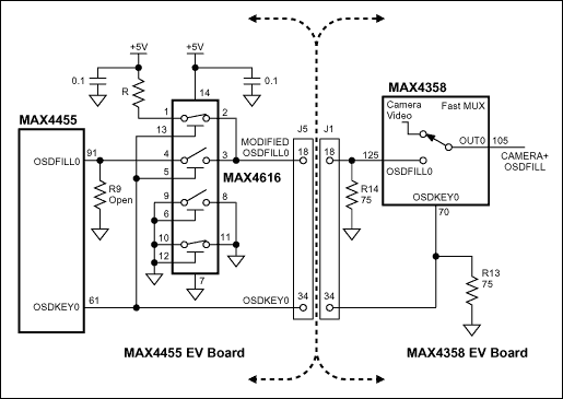
Figure 2. Modification to the MAX4455 EV circuit board on channel 0.
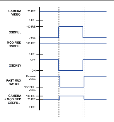
Figure 3. Fix for the finite switch time effect.


 关注微信
关注微信