The dual, voltage-output
DACs shown in the figure below employ a combina
tion of power-conserving tr
icks to draw less than 20µA from a 5V supply. The circuit suits a need f
or prog
rammable voltage generation in slow or static applications, such as the nulling of offsets in a micropower instrument.
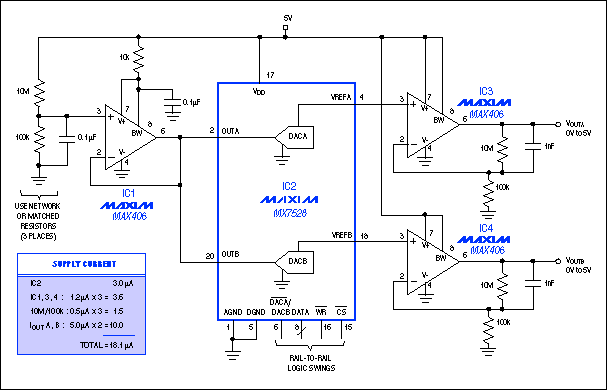
Providing two independent 8-bit DACs with voltage outputs and a common reference, this dual-DAC circuit draws less than 20µA from a 5V supply.
Current-output DACs normally waste power by routing the complement of IOUT to ground. The circuit in the figure avoids wasting power by operating e
ach DAC in the reverse voltage-switching mode, in which the reference voltage is applied to the
pins normally labe
led IOUT.
The OUT pins in this circuit have a constant and relatively low input imp
edance of 11kΩ. To reduce input currents, the reference voltage is divided by 100 (from 5V to 50mV) and therefore delivers only 5µA to each DAC input. Signal levels are restored by a compensating g
ain of 100 in each output amplifier. Inexpensive 10MΩ/100kΩ resistor networks are a good choice for the multiple 100:1 at
tenuators required. Though only 2% accurate, their matching and tracking is much better than that of discrete resistors.
Greater scaling is impractical because of 0.5mV (
maximum) offsets in the output amplifie
rs shown. Amplified by 100, these offsets produce worst-case output errors of ±1% (0.05V). The errors are constant over temperature, but
additional error due to drift over a range of 40°C is typically ±½LSB. The micropower output amplifiers shown in the figure were chosen for their low supply current—their typical IDD is only 1µA.
The last requirement for minimizing the overall current drain is to ensure that
logic signals applied to the digital inputs of IC1 swing to within 0.2V of each rail. The maximum specified IDD for that condition is 100µA over temperature, but this specification (like most CMOS IDD ratings) is extremely conservative. IDD is negligible for Rail-to-Rail swings but rises
dramatically as the swings approach TTL levels.


 关注微信
关注微信