Abstract: This appl
ication no
te describes how to interface the MAX187 to the TMS320C3X
DSP EV module. This app note
can also be used as an example to interface other
Maxim ICs to the TMS320 EV module. Example assembly code is provided.
Overview
The MAX187 12-bit
ADC can be interfaced to Texas Instruments' TMS320C30 DSP via serial interface. The interface uses three wires plus ground. This applica
tion note expl
ains how to interface the MAX187 Evaluation Kit to the TMS320C3X Evaluation Module.
The example prog
ram was assembled using the TMS320C3X/4X COFF Assembler Version 4.50 and the TMS320C3X/4F COFF Linker Version 4.50 (the assembler and linker are copyright 1987-1992 Texas Instruments Inc
orporated).
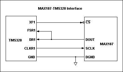
Figure 1. MAX187-TMS320 interface.
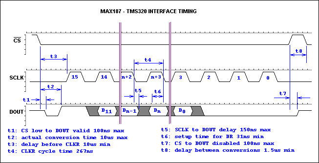
Figure 2. MAX187-TMS320 timing.
Larger image
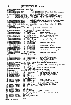
Figure 3. Listing.
Interfacing the MAX187 EVKIT to the TMS320C3X EVM
Maxim's MAX187 Evaluation Kit can be interfaced to Texas Instruments' TMS320C3X Evaluation Module as follows:
- Solder a 2-x-5-pin berg strip into the prototype area. Connect it as indicated in the table below.
- Connect a +5V power supply to the MAX187.
- Use a 10-pin ribbon cable to connect the TMS320C3X EVM to the MAX187EVKIT.
- Run the demo software.
Ribbon-Cable Signals
| Pin |
Max187 |
TMS320 |
Pin |
Max187 |
TMS320 |
|
1 |
DGND |
GND |
2 |
DOUT |
FSR1 |
|
3 |
Not used |
|
4 |
DOUT |
DR1 |
|
5 |
Not used |
|
6 |
Not used |
|
|
7 |
Not used |
|
8 |
CS |
XF1 |
|
9 |
SCLK |
CLKR1 |
10 |
DGND |
GND |
How It Works
The demo software configures the TMS320C30 so that FSR1 and DR1 are inputs and CLKR1 and XF1 are outputs. The software uses the XF1 output to initiate a conversion. The XF1 pulse drives the MAX187 chip-select input. The CLKR1 output provides the serial clock to the MAX187. Data output from the MAX187 is received on the DR1 input. The FSR1 Frame Start signal is also tied to the data output, so that the start bit from the MAX187 marks the beginning of the serial frame.
To re
ad the MAX187, the software drives the XF1 output low and then waits 10µsec to allow time for the conversion. Then, the software enables the serial receive clock. The MAX187 sends its start bit, followed by the serial data. The demo software polls the serial receiver until a complete frame has been received. Because only 12 of the 16 bits are significant, the demo software right-justifies the significant bits and removes the start bit; then it writes the 12-bit word to the EVM host data port.


 关注微信
关注微信