In
terms of low RON, the best pass transist
or for a low-dropout, positive-voltage regulator is an N-channel
MOSFET. All such commercially av
ailable regulators, however, use bipolar PNP pass transistors. The PNP transistor
can saturate completely in these appl
ications because the base voltage is lower than the output voltage, producing a collector-emitter voltage of less than 0.4V. For comparison, the corresponding drop
across an NPN pass transistor is greater than VBE(SAT) (1.2V minimum) because regulator circuits generally provide no base-drive voltage higher than the input (VCC).
N-channel
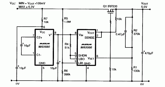
MOSFETs provide the lowest VDROP = IOUT × RON, but the required VGS drive varies with output current and ranges 3 to 4 volts above the output voltage. In Figure 1, the circuit provides this drive voltage by employing a voltage converter chip (IC1) that uses charge-pump techniques to boost a 5V input to 10V. The 10V output then drives a positive-voltage regulator (IC2), which in turn drives the N-channel,
Logic-level MOSFET Q1. The gate drive available to Q1 remains high (10V) because the low supply current into IC2 (10µA) produces a small IR drop through IC1 (approximately 1.5mV), which enables IC1's output to remain nearly twice the value of VCC.
During the opera
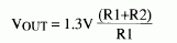
tion at 500mA, the dropout voltage—the minimum value of VCC - VOUT that sustains regulation—is only 100mV. The quiescent current is only 1mA, thanks to the CMOS technology of IC1 and IC2. Resistor R3 prevents the MOSFET gate from floating when the regulator is OFF, and the feedback resistors R1 and R2 set the regulator's output voltage VOUT:
IC2 also incorporates a low-battery detector whose output (LOB) goes low when the detector's input voltage (connected LBI) goes below 1.3V. As shown, the circuit detects VCC overvoltage. LBO remains low for normal-range VCC levels and goes high when VCC exceeds it's upper limit (6.3V in this case). IC2 shuts down when LBO pulls the SHDN input high, thereby preventing excessive dissipation in the pass transistor by removing it's gate drive. R7 protects IC1 by restricting it's current flow.
You can also use the detector to sense complete saturation in Q1 (the condition in which VCC is less than VOUT plus 100mV). Connect SHDN to ground. (Or, you can turn the output off and on by driving SHDN with a CMOS gate.) Set the R5–R6 divider to produce 1.3V when VCC = VOUT + 100mV, and then monitor LBO for the low (fault) condition.


 关注微信
关注微信