时间:2009-05-03 14:33
人气:
作者:admin
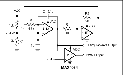
Figure 1. This 3-op-amp circuit produces a triangular wave and a variable-pulsewidth output.
The circuit consists of a triangle-wave generator (U1A and U1B) and a comparator (U1C). U1A is configured as an integrator (or de-integrator), and U1B as a comparator with hysteresis. At power-up, the comparator's output voltage is assumed to be zero.
U1A's non-inverting input is biased at VCC/2. A virtual connection between the inverting and non-inverting inputs allows a constant current through R equal to I = VCC/2R, which charges the capacitor C. Thus, the U1A integrator output increases linearly with time. When it reaches 0.75VCC, the comparator output (U1B) changes to its maximum output voltage (VCC). At that point the integrator begins to de-integrate, causing the output voltage to decrease linearly. When it reaches 0.25VCC the comparator output voltage changes to zero, and the cycle repeats. Thus, the integrator output is a triangular wave that swings between the levels of ¼ VCC and ¾VCC.
U1C compares the triangular wave against the dc level VIN. Its output is a square wave, with a duty cycle that varies from 0% to 100% as VIN varies from ¼ VCC to ¾ VCC (Figure 2). Frequency is determined by R, C, R1, and R2:
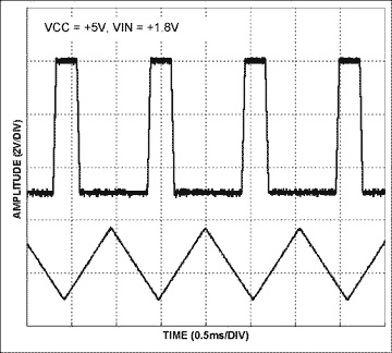
Figure 2. The Figure 1 circuit produces these PWM and triangular-wave outputs.
The ratio of R2 and R1 affects the operating frequency and the amplitude of the triangular wave. Given that VTH is the triangular wave's maximum voltage and VTL is its minimum voltage, the amplitude swing is:
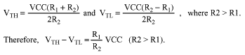
The triangular wave's peak-to-peak voltage (the difference in its maximum and minimum voltages) is centered at the VCC/2 bias voltage generated by R3 and R4. The circuit configuration shown allows the PWM to operate on a single supply. Use micropower op amps and larger resistors (R and R1 - R4) for low-power applications, and high-frequency op amps for higher-frequency applications. (The quad op amp shown comes in a single package.)


 关注微信
关注微信