Addi
tional Inf
ormation:
- Quick View Data Sheet for the MAX828/MAX829
- Technical Support: Power
In telecom applications, particularly the rectifier applications (or front-end power supplies), a negative reference voltage is needed for primary-side control circuitry (op amps) to increase common-mode noise immunity. The value is about 2V to 3V without regulation. Power consumption of the negative voltage is negligible. A
simple way to realize such a negative reference voltage is by using a three-
diode voltage drop (see Figure 1).
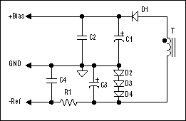
Figure 1. A typical discrete appro
ach to generate negative reference voltage.
This circuit, at fi
rst glance, appears to be a simple and cheap solution. However, in practice, it is not inexpensive for the following reasons: (1) The diodes D2 to D4 must have the same current rating as D1. This is because these diodes carry the same current as D1, even though the current sourced by -Ref is negligible. (2) Because of large-ripple current passes through D2, D3, and D4, the voltage ac
ross the three diodes is not constant; therefore, a large value of the capacitor (C3, around 47µF) is needed to filter out the ripple voltage. To have smoother negative reference voltage (less than 300mV ripple), another filter (R1 and C4) is required. (3) Particularly when the cooling fan is powered from the primary side, extra power dissipation in the three diodes causes a thermal problem on these diodes at high ambient temperatures. In addition, these components occupy more space and increase manufacture cost. Therefore, a simple and space-saving solution is needed for reduced power dissipation to increase bias-supply reliability.
Figure 2 shows a simple solution that uses
Maxim's space-saving and highly efficient charge-pump product, the MAX828/829. The MAX828 is designed for 0°C to +75°C and the MAX829 for -40°C to +85°C.
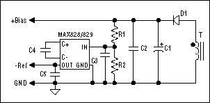
Figure 2. -Ref circuit employing the MAX828/829 charge-pump IC.
Note that R1 and R2 are resistor dividers in case the primary bias voltage is more than 5.5V. C3 is the filtering capacitor. If the primary-side bias voltage is less than 5.5V, these components
can be omitted. Advantages of such implementation for negative reference voltage are as follows: (1) Space saving. As -Ref sources only a few mini ample currents, the capacitors, C3, C4, and C5 can be 0603 in size and the resistors R1 and R2 can be 0804 in size. The MAX828/829 come in a tiny SOT23-5 package. (2) High reliability. This is because power dissipation in the negative reference circuit is very small. (3) -Ref is not temperature-dependent anymore. In previous implementations, the diode voltage drop was a function of both the temperature and the load current.
An Example: For a -5V/2mA negative reference voltage from +12V primary bias, R1 = 1k, R2 = 910Ω, C3 = C4 = C5 = 0.022µF/16V (0603). At 2mA output current, the efficiency is about 90% (from the data sheet).


 关注微信
关注微信