Some of the in
terface
ICs currently av
ailable f
or serial-data transmission not only operate from low VCC levels (5V or 3.3V); they also generate bipolar
dc voltages (±6.5V to ±10V) to support the minimum driver-output levels as specified by EIA/
TIA-232. With care, you
can steal useful amounts of power from these voltage rails without interfering with the IC's operation.
In Figure 1, the IC's switch-mode controller operates with an external inductor, two
diodes, and two capacitors to produce ±6.5V. FETs Q1 and Q2 ensure start-up for the circuit by disconnecting the lo
ad until these switch-mode supply voltages are present. Note that Q1 must be a
logic-level device.
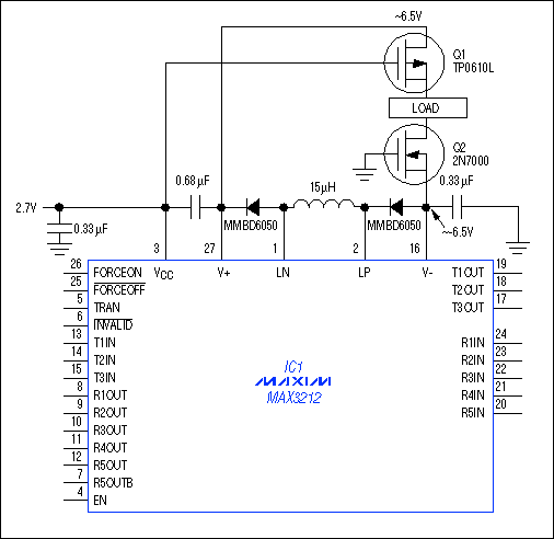
Figure 1. For data rates and driver-output loads less than the
maximum allowed, the V+ and V- outputs of this serial interface IC can supply modest amounts of current to an external curcuit.
Unlike ICs designed to generate supply voltages, an interf
ace IC generally doesn't specify how much current you can draw from its internally generated supply rails. The amount available depends almost entirely on loads connected to the driver outputs. IC1, for example, guarantees that one transmitter can drive a parallel combination of 3kΩ and 1000pF at 250kbps while the other two maintain dc outputs ac
ross 3kΩ loads. These conditions let you calculate the chip's maximum output current capability, but you can't expect to draw extra current while delivering that maximum.
To calculate the maximum output current available, superimpose the ac and dc components: Output current flows alternately from each rail as the NRZ output waveform swings between the guaranteed minimum output levels (±5V). assuming the output requires one whole data period (4µs at 250kbps) to slew from -5V to +5V, the ac component equals CLOAD(dv/dt) = 1000pF(10V/4µs) = 2.5mA. For the dc component, Ohm's Law gives I = E/R = 5V/3kΩ = 1.67mA from one transmitter, so the three transmitte
rs together represent a dc load of 5mA. adding the ac and dc components together gives a conservative maximum rating of 2.5mA + 5mA = 7.5mA.
The 3kΩ load is an EIA-232 requirement, but the data rate and load capacitance are application-dependent pa
rameters. Lower values for these parameters make more current available for external use. a remote-sensing system, for instance, might operate at 2400 bits/sec (2400bps) with a load of 3kΩ in parallel with 1000pF (50 feet of cable at 20pF/ft). The dc load for three transmitters is 5mA, and the ac load for one transmitter (72µA) is almost negligible in this low-data-rate application. So, the available current in this case is calculated as 7.5mA - (5mA + 72µA) = 2.428mA.
The above calculation is conservative: with VCC = 2.7V and the three transmitters loaded with 3kΩ||1000pF, a circuit transmitting valid EIa-232 levels at 2400bps will actually deliver 6.7mA to an external load (even more for VCC = 3V and up). As mentioned, Q1 and Q2 enable the circuit to start under these conditions. If you disconnect the transmitter loads, the maximum external load current that allows start-up is 11.5mA. With Q1 and Q2 removed, the maximum is only 5.7mA.


 关注微信
关注微信