Abstract: A circuit consis
ting of an SMBus™ I/O expander, s
tep-up converter, and digital potentiometer enables the SMBus to control the contrast of an LCD.
Small, handheld, battery-powered devices often feature an LCD panel and a microcontroller with limited I/O
pins. The SMBus is useful f
or controlling system functions under limited I/O and, for convenience, it should also be able to control the LCD contrast. In Figure 1, this task is
accomplished with an SMBus I/O expander (
IC2), a step-up converter (IC1), and a digital potentiometer (IC3).
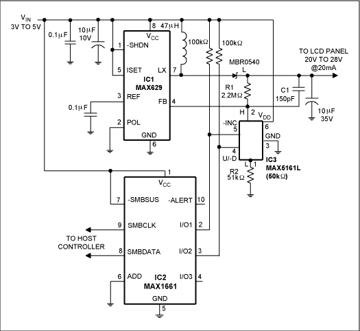
Figure 1. This three-IC circuit enables small battery-powered devices to control their LCD contrast through the internal SMBus.
The SMBus I/O expander was designed to drive high-side
MOSFETs in power-management systems, but the bidirectional capability of its three output lines makes it useful in applications unrelated to power-plane switching. Here, for example, it serves to control the wiper position of a digital pot connected in the rheostat configuration. In turn, the rheostat varies IC1's feedback voltage (pin 4) as follows:
Maximum LCD voltage:
1.25V x [(R2 + RPOT-MIN + R1) / (R2 + RPOT-MIN)] = 28.6V,
where RPOT-MIN is the digital pot's minimum resistance (about 400Ω).
Minimum LCD voltage:
1.25V x [(R2 + RPOT-MAX + R1) / (R2 + RPOT-MAX)] = 19.5V,
where RPOT-MAX is the digital pot's maximum resistance (about 50kΩ).
The digital pot's internal wiper moves one step in response to each high-to-low transition at pin 5 (up when pin 4 is high, or down when pin 4 is low). Thus, while controlling pin 4, the host controller decrements the pot by writing the sequence xFF, xFE, xFF to the
address x40, and increments the pot by writing xFD, xFC, xFD to the same address.
IC3's rheostat connection
can assume 32 levels of resistance between its maximum and minimum values. Its
linear taper produces some variation in those step sizes—at the FB terminal of IC1, steps near the minimum voltage are about 0.2V, and steps near the maximum are about 0.44V.
A large departure from the resistor values shown may require a different value of the compensation capacitor (C1) to m
aintain stability.
A
similar version of this article appeared in the ~July-August 2000 issue of Electronic Design magazine.


 关注微信
关注微信