时间:2009-04-23 14:21
人气:
作者:admin
V+(MIN) = (VPORT + VLED) volts
where VPORT is the voltage drop across the output port when sinking the required load current (0.6V at 24mA for MAX6956 and MAX6957)
VLED is the voltage drop across the LED(s) at the required load current (usually in the range 1.8V to 2.4V for red LEDs, and 3V to 4.2V for blue, white, and high efficiency green LEDs).
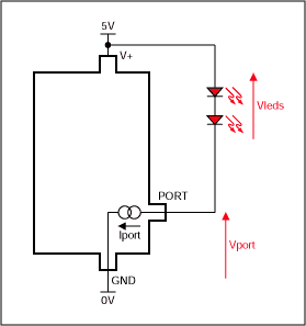
Figure 1. Standard LED connection.
Figure 1 shows the LED output load returned to the driver supply voltage. This is usually the most convenient load supply. However, the load can be connected to a lower voltage instead if desired. A good reason to use a lower voltage LED supply is to improve efficiency and reduce driver dissipation by better matching the LED forward voltage with the supply. The example shown in Figure 2 demonstrates an RGB triad driven using the driver 5V supply as the supply for the high forward voltage blue and green LEDs, and a 3.3V supply for the low forward voltage red LED.
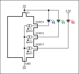
Figure 2. Connecting LEDs to multiple supplies.
Loads must not be connected to a voltage higher than the MAX6956's or MAX6957's chip supply V+ because these output ports are not over-voltage protected. Take care to consider the power-up sequencing when using different supplies for driver and load to avoid an output being pulled up higher than chip supply. This would happen in the Figure 2 circuit if the 3.3V supply powered up before the 5V supply.
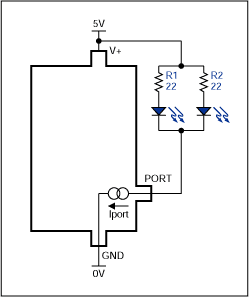
Figure 3. Driving multiple LEDs from one output.
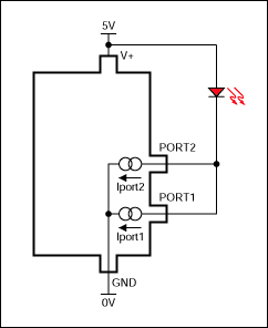
Figure 4. Paralleling outputs to increase drive current.
The circuit shown in Figure 5 uses a single transistor level shifter to allow a higher voltage to be used to drive the LEDs, while retaining the LED driver output's constant current behavior. Q1 operates as a common-base (cascode) current switch. The port output VPORT is constrained to a safe voltage of (V+ - VBE) because Q1's base is tied to the driver supply voltage, V+. The port's constant current Iport will flow through Q1's collector and the LED loads, less a small base current taken by Q1. The current error due to Q1's base current can be kept below 1% by choosing a reasonably high gain (ß > 100) transistor for Q1.
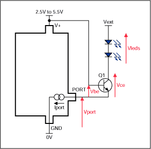
Figure 5. Driving LEDs from a higher voltage.
The lowest that the collector of transistor Q1 can go is (V+ - VBE + VCE) volts, or about (V+ - 0.5V). The maximum drive voltage available for the LEDs is therefore (VEXT - V+ + 0.5V) volts. The MAX6956 or MAX6957 will dissipate (Vport x Iport) = ((V+ - VBE) x Iport) watts for that output, independent of the LED supply voltage Vext. The pass transistor Q1 will absorb the excess LED supply voltage not dropped across the LEDs, and therefore will dissipate ((VEXT - VLEDS - V+ + VBE) x IPORT) watts.
For more drive current as well as higher voltage, combine the circuits of Figures 4 and 5. Parallel as many ports are needed (2 are shown paralleled in Figure 4) connected to the emitter of a single pass transistor as shown in Figure 5. Only one external pass transistor is needed, rated for the total current of all the paralleled ports.
A limitation of the circuit shown in Figure 5 is that the collector of Q1 can go no lower than (V+ - VBE + VCE(sat)), which is only a little below V+. If V+ is high, for example 5V, then not only is the MAX6956 or MAX6957 dissipating a high power due to this high voltage drop forced across its output, but also the voltage headroom available for the LEDs is reduced. A simple solution is to bias Q1's base to a lower voltage using a series zener diode. Only one zener diode is needed to serve multiple pass transistors, as shown in the example circuit in Figure 6. With this circuit the MAX6956 or MAX6957 drops about 1.5V to 2.5V as the supply voltage varies from 4.5V to 5.5V.
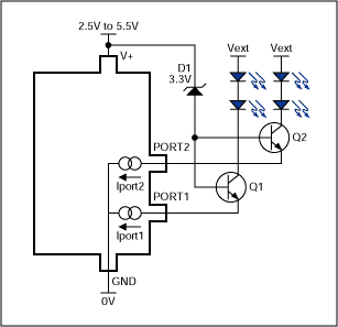
Figure 6. Using a zener diode to minimize driver headroom.
See Als
Driving LEDs with open drain port expander outputs
Driving LEDs with push-pull port expander outputs


 关注微信
关注微信