Abstract: This appl
ica
tion no
te will help the user of the Dallas Semiconductor secure microcontroller and high-speed microcontroller improve reliability when implementing nonvolatile S
RAM. This note is applicable to the Secure and High-Speed Secure Microcontroller families as well as the DS87C530 high-speed microcontroller. Out-of-tolerance voltage s
pikes, protecting I/O pins and negative power supply transients are discussed in this application note.
Overview
Microcontrolle
rs which inc
orporate battery-b
acked, nonvolatile SRAM (NV RAM) have found wide acceptance in the embedded marketplace. Unlike Flash memory or EEP
ROM technology, nonvolatile SRAM has no write limitations, which makes it ideal for real-time data logging applications. In products such as the Dallas Semiconductor Secure Microcontroller family, NV RAM
can be used to provide insystem reprogrammable program memory.
This application note discusses design guidelines for microcontroller products which incorporate NV RAM. A number of design suggestions are presented to improve the reliability of microcontrollers which incorporate NV RAM. It should be stressed that battery-backed memory is as reliable as nonvolatile memory as long as standard CMOS design guidelines are used. This application note is applicable to the Secure and High-Speed Secure Microcontroller family of products as well as the DS87C530 High-Speed Microcontroller.
Out-of-Tolerance Voltage Spikes
The real world is a harsh place; electrostatic discharge (
ESD), electrical noise, etc. can enter into a system. Many of these phenomena can induce negative voltages on one or more device pins. CMOS design guidelines require that no pin be taken above VCC or below VSS. Violation of this guideline can result in a hard failure (damage to the silicon inside the device) or a soft failure (unintentional modification of memory contents).
Negative voltage spikes are a particular problem for CMOS devices. When a negative voltage spike is experienced, one or more parasitic
diodes inside the device can become forward-biased. This will cause the device to consume a large amount of current, and can cause the device to latch-up. In general, the only way to reverse CMOS latch-up is to remove power from the device. If the supply to the device is not limited, the excessive current draw can cause irreparable damage to the device.
Less severe, but just as troublesome, is the effect this can have on nonvolatile memory. When a parasitic diode forms, a high-current path will form. This will dr
ain current away from the device, and may cause the voltage to sag internally. If the internal voltage drops below the minimum needed to maintain the memory, soft errors may be experienced.
In a practical application, it is often difficult or impossible to remove all voltages above VCC or below VSS. Realistically, overshoots or undershoots of 0.3V can be tolerated by most devices. The following cases discuss common causes of such conditions and ways to minimize their effect on systems.
Protecting I/O Pins
The most common way that a device experiences negative voltage spikes is through its general-purpose I/O pins. These are usually the only contact that the microcontroller has with the "outside world." Devices such as electrical motors and key
pads can generate large amounts of electrical noise. The shock that one experiences when touching a doorknob, for example, can be as much as 30kV. If this voltage is transmitted from a keypad into a microcontroller system, it can seriously damage electronic components.
Figure 1 demonstrates a diode protection scheme that can be used to protect the I/O pins of a microcontroller. The scheme relies on the use of a Schottky diode and current limiting resistor to reduce the effect of current spikes on the device. When the voltage approaching the device pin exceeds VCC or VSS by more than 0.1V - 0.2V, the Schottky diodes will become forward biased, conducting the excess voltage away from the device pins. The current limiting resistors will also help dampen the effect of the voltage spike on the microcontroller.
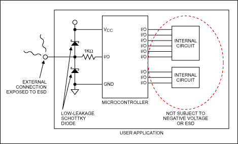
Figure 1. External I/O protection scheme.
The protection diodes shown in Figure 1 must be chosen carefully. Most Schottky diodes, such as the popular 1N5817, are suitable at room temperature. At high temperatures, however, their reverse bias leakage will begin to lo
ad the I/O line, making it difficult for the device to drive a
logic 1. For example, a DS87C520 can drive a logic 1 with a
maximum current of 50µA. At room temperature, the reverse leakage of a typical 1N5817 is 30µA. At 70°C, however, the reverse leakage is greater than 100µA. The microcontroller will be unable to source enough current to maintain a CMOS logic high of 2.4V.
Any Schottky diode used should have a leakage well below the maximum drive current of the sourcing device. Diodes with low reverse leakage currents are available from many vendors.
Negative Power Supply Transients
Another source of voltage spikes is the power supply. Many
simple voltage regulators, such as a 7805 5V regulator, are notorious for generating voltage spikes as they power up. Care must be exercised when designing the power supply so that it does not generate excessive noise when powering up or when switching loads in and out of the system.
The problem of power supply transients can be lessened by using a reverse-biased Schottky diode ac
ross VCC and GND, similar to that used for protecting I/O pins. Figure 2 shows one such scheme.
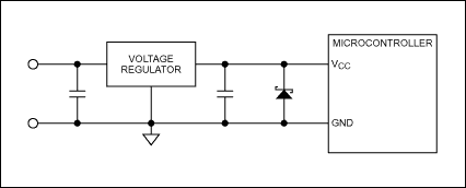
Figure 2. Voltage regulator protection scheme.


 关注微信
关注微信