Abstract: This appl
ica
tion no
te provides general inf
ormation about how to interface a real-time clock (RTC) that has a multiplexed-bus (multiplexed
address and data) interface (example: DS12887) with a microcontroller that has separate address and data buses.
An IC multiplexed-bus real-time clock (RTC) is designed for use with processo
rs that include a multiplexed data-address bus, but some designers prefer to use such "mux-bus" RTCs with processors whose data and address buses are separate (Figure 1).
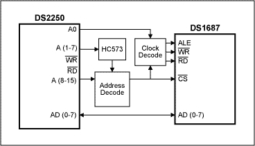
Figure 1. The components shown interface a mux-bus RTC to a processor (DS2250) with separate data and address buses.
The mux-bus RTC has four control signals. Chip Select (
active-low CS) must be active when re
ading or writing data. Read Data strobe (active-low RD) is for data reads, Write Data strobe (active-low WR) is for data writes, and Address Strobe (ALE) latches the register address internally. The falling edge of ALE latches the register address (presented on
pins AD0-AD7 of the Address/Data bus) whenever active-low RD and active-low WR are both high. You then transfer data to or from the selected clock register via AD0-AD7 by toggling active-low WR or active-low RD low while active-low CS is active.
In Figure 1, the interface between the RTC (DS1687) and an 8051-type processor (DS2250) ignores the expanded memory multiplexed address and data function provided by the processor's P0, P2 and ALE pins (not shown). Instead, external
logic creates the ALE signal, and the RTC is memory-mapped into the expanded memory area.
The configuration above requires two address locations in the processor address space. When A0 is low, the clock-decode logic toggles ALE while active-low RD and active-low WR are held high. When A0 is high, the clock-decode logic holds ALE low while toggling active-low RD or active-low WR low. The address-decode logic holds active-low CS low for either state of A0, provided A1-15 matches the address to which the clock is mapped. In software, you access the clock by writing the register address to the lower address (A0 low), which is followed by a read or write to the upper address (A0 high). The associated software
can be downloaded from the
Maxim site. Figure 2 shows the complete schematic.
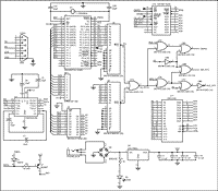
For Larger Image
Figure 2.


 关注微信
关注微信