Abstract: How to interface the DS2172/DS21372 BERT to all Dallas Sem
iconductor family of T1/E1 frame
rs and single-chip transceivers (SCTs).
Introduction
This application no
te shows a how to connect a Dallas BERT to a Dallas framer/single-chip transceiver (SCT). This application note applies to the following products:
| T1 Framers |
E1 Framers |
T1 SCTs |
E1 SCTs |
T1/E1 SCTs |
| DS2141 |
DS2143 |
DS2151 |
DS2153 |
DS2156 |
| DS21Q41 |
DS21Q43 |
DS2152 |
DS2154 |
DS2155 |
| DS21Q42 |
DS21Q44 |
DS21352 |
DS21354 |
DS21Q55 |
| DS21FF42 |
DS21FF44 |
DS21552 |
DS21554 |
DS21455 |
| DS21FT42 |
DS21FT44 |
DS21Q552 |
DS21Q554 |
DS21458 |
| |
|
DS21Q352 |
DS21Q354 |
|
General Configuration
The circuit in Figure 1 describes a method of interfacing the DS2172/DS21372 bit err
or-rate tester (BERT) to the Dallas Semiconductor family of T1/E1 f
ramers and single-chip transceivers. This diagram illustrates how the BERT
can be used in a real system with the use of a multiplexer to determine whether to put the system in test mode and use the BERT or to disable the BERT and send normal data. The receive side of the DS2172/DS21372 can be connected directly to the receive-data stream of the framer/SCT. The DS21372 is a 3.3V version of the DS2172.
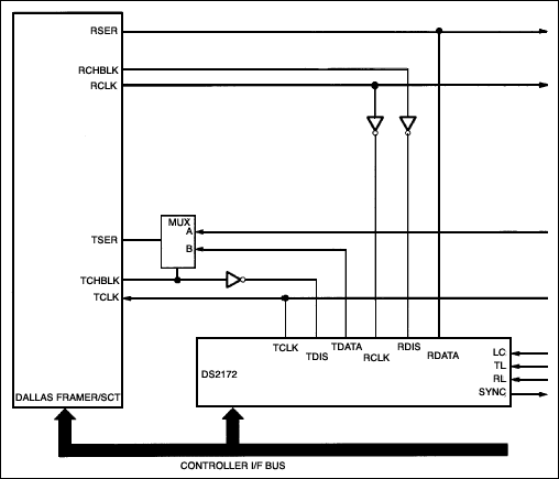
Figure 1. Framer/SCT to DS2172/DS21372 interface.
The RCHBLK and TCHBLK outputs from the framer/SCT are used to determine the time slot or band in which the BERT is to transmit or receive data. These
pins are programmed using the RCHBLK/TCHBLK registers. The RCHBLK/TCHBLK pins are normally low; writing the register bits to one will set the pin to a high voltage during that time slot. In this configuration, setting the RCHBLK and TCHBLK pins high enables the DS2172/DS21372 to transmit and receive data.
Figure 1 shows the DS21x5y with the elastic stores disabled. If the elastic stores are enabled, the user will use the system clock (TSYSCLK, RSYSCLK) as inputs to the DS2172/DS21372 rather than RCLK and TCLK.
Note: In T1 framers/SCTs, the TCHBLK/RCHBLK pin cannot be configured to be high during the F-bit position. This means the DS2172/DS21372 cannot source data during the F-bit position of e
ach frame. E1 framers/SCT TCHBLK/RCHBLK can be programmed to be high during the entire frame. Listed below are the TCHBLK/RCHBLK registers for any E1 framer or any E1-only SCT listed above.
RCBR1/RCBR2/RCBR3/RCBR4: Receive-Channel Blocking Registers
Address
(2B to 2E Hex) |
(MSB) |
|
|
|
|
|
|
(LSB) |
| RCBR1 (2B) |
CH8 |
CH7 |
CH6 |
CH5 |
CH4 |
CH3 |
CH2 |
CH1 |
| RCBR2 (2C) |
CH16 |
CH15 |
CH14 |
CH13 |
CH12 |
CH11 |
CH10 |
CH9 |
| RCBR3 (2D) |
CH24 |
CH23 |
CH22 |
CH21 |
CH20 |
CH19 |
CH18 |
CH17 |
| RCBR4 (2E) |
CH32 |
CH31 |
CH30 |
CH29 |
CH28 |
CH27 |
CH26 |
CH25 |
| Name |
Position |
Function |
| CH1µ32 |
RCBR1.0µ4.7 |
Receive-Channel Blocking Control Bits
0 = force the RCHBLK pin to remain low during this channel time
1 = force the RCHBLK pin high during this channel time |
TCBR1/TCBR2/TCBR3/TCBR4: Transmit-Channel Blocking Registers
Address
(22 to 25 Hex) |
(MSB) |
|
|
|
|
|
|
(LSB) |
| TCBR1 (22) |
CH8 |
CH7 |
CH6 |
CH5 |
CH4 |
CH3 |
CH2 |
CH1 |
| TCBR2 (23) |
CH16 |
CH15 |
CH14 |
CH13 |
CH12 |
CH11 |
CH10 |
CH9 |
| TCBR3 (24) |
CH24 |
CH23 |
CH22 |
CH21 |
CH20 |
CH19 |
CH18 |
CH17 |
| TCBR4 (25) |
CH32 |
CH31 |
CH30 |
CH29 |
CH28 |
CH27 |
CH26 |
CH25 |
| Name |
Position |
Function |
| CH1µ32 |
TCBR1.0µ4.7 |
Transmit-Channel Blocking Control Bits
0 = force the TCHBLK pin to remain low during this channel time
1 = force the TCHBLK pin high during this channel time |
Listed below are the TCHBLK/RCHBLK registers for any T1 framer or any T1-only SCT listed above.
RCBR1/RCBR2/RCBR3: Receive-Channel Blocking Registers
Address
(6C to 6E Hex) |
(MSB) |
|
|
|
|
|
|
(LSB) |
| RCBR1 (6C) |
CH8 |
CH7 |
CH6 |
CH5 |
CH4 |
CH3 |
CH2 |
CH1 |
| RCBR2 (6D) |
CH16 |
CH15 |
CH14 |
CH13 |
CH12 |
CH11 |
CH10 |
CH9 |
| RCBR3 (6E) |
CH24 |
CH23 |
CH22 |
CH21 |
CH20 |
CH19 |
CH18 |
CH17 |
| Name |
Position |
Function |
| CH1µ24 |
RCBR1.0µ3.7 |
Receive-Channel Blocking Control Bits
0 = force the RCHBLK pin to remain low during this channel time
1 = force the RCHBLK pin high during this channel time |
TCBR1/TCBR2/TCBR3: Transmit-Channel Blocking Registers
Address
(32 to 34 Hex) |
(MSB) |
|
|
|
|
|
|
(LSB) |
| TCBR1 (32) |
CH8 |
CH7 |
CH6 |
CH5 |
CH4 |
CH3 |
CH2 |
CH1 |
| TCBR2 (33) |
CH16 |
CH15 |
CH14 |
CH13 |
CH12 |
CH11 |
CH10 |
CH9 |
| TCBR3 (34) |
CH24 |
CH23 |
CH22 |
CH21 |
CH20 |
CH19 |
CH18 |
CH17 |
| Name |
Position |
Function |
| CH1µ24 |
TCBR1.0µ3.7 |
Transmit-Channel Blocking Control Bits
0 = force the TCHBLK pin to remain low during this channel time
1 = force the TCHBLK pin high during this channel time |
Conclusion
This application note has shown how to connect our framers/SCTs to our DS2172/DS21372 BERT.
If you have further questions about connecting any of our framers/SCTs to our BERTs, then please contact the Telecommunication Applications support team via em
ail
telecom.support@dalsemi.comor call 972-371-6555.
Dallas Framer/SCT And BERT Information


 关注微信
关注微信