Abstract: Appl
ica
tion no
te 310 cont
ains inf
ormation necessary to control D4 f
raming and signaling on the Dallas Semiconductor T1 devices. It incorporates the necessary information to enable both transmit and receive D4 framing and signaling. For the transmit path, programming of the registe
rs for framing and signaling operations are discussed in detail. For the receive path, programming of the registers for recovering framing and signaling is discussed along with receive interrupt handling. The application note provides all the necessary information to get the Dallas Semiconductor T1 device operating in D4 mode.
Introduction
This application note applies to the following products:
| T1 Framers |
T1 SCTs |
| DS2141A |
DS2151 |
| DS21Q41B |
DS2152 |
| DS21Q42 |
DS21352 |
| DS21FF42 |
DS21552 |
| DS21FT42 |
DS21Q352 |
| |
DS21Q352 |
All Dallas Semiconductor T1 framers and single-chip transceivers (SCTs) provide support for D4 framing and signaling, as shown in Figure 1. This application note provides the requirements to enable the D4 format in the transmit and receive paths for T1 framers and SCTs.
For the transmit path, programming the registers for framing and signaling operations are discussed. For the receive path, programming the registers to retrieve framing and signaling is discussed along with receive interrupt handling.
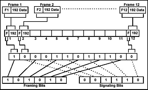
Figure 1. D4 framing format.
D4 Framing Register Settings
Several registers must be initialized to enable D4 multiframing. Table 1 shows the register settings required to generate and receive D4 multiframing.
Table 1. D4 Framing Register Settings
| Register Setting |
Function |
| CCR2.7, CCR2.3 = 0 |
Selects D4 multiframing in the transmit and receive directions. |
| CCR2.5 = 1 |
Enables insertion of the 6-bit Fs pattern. |
| TFDL = 1Ch |
This is the 6-bit Fs pattern. |
| RCR1.3 = 1 |
If this bit is cleared, the receiver declares synchronization on the Ft pattern only and will not be guaranteed to find the D4 multiframe boundary. |
| Toggle low to high RCR1.0 |
Required after configuring the control registers to force resynchronization. |
Transmit Signaling Registers
In D4 multiframing, only six of the 12 transmit signaling registers are needed to lo
ad a multiframe of signaling. The transmitter alternates, lo
ading the contents of TS1 through TS6 into one multiframe, followed by the contents of TS7 through TS12 into the next multiframe, then b
ack again. Therefore, load the transmit signaling bytes into two registers, as shown in Table 2. A full register map shows the bits of each transmit signaling register in Table 3.
Table 2. Transmit Signaling Registers
| Register |
Description |
| TS1 and TS7 |
A bits for channels 1 through 8 |
| TS2 and TS8 |
A bits for channels 9 through 16 |
| TS3 and TS9 |
A bits for channels 17 through 24 |
| TS4 and TS10 |
B bits for channels 1 through 8 |
| TS5 and TS11 |
B bits for channels 9 through 16 |
| TS6 and TS12 |
B bits for channels 17 through 24 |
Table 3. Transmit Signaling Register Map (D4 Format)
|
(MSB) |
|
(LSB) |
| TS1 (70h) |
CH8-A |
CH7-A |
CH6-A |
CH5-A |
CH4-A |
CH3-A |
CH2-A |
CH1-A |
| TS2 (71h) |
CH16-A |
CH15-A |
CH14-A |
CH13-A |
CH12-A |
CH11-A |
CH10-A |
CH9-A |
| TS3 (72h) |
CH24-A |
CH23-A |
CH22-A |
CH21-A |
CH20-A |
CH19-A |
CH18-A |
CH17-A |
| TS4 (73h) |
CH8-B |
CH7-B |
CH6-B |
CH5-B |
CH4-B |
CH3-B |
CH2-B |
CH1-B |
| TS5 (74h) |
CH16-B |
CH15-B |
CH14-B |
CH13-B |
CH12-B |
CH11-B |
CH10-B |
CH9-B |
| TS6 (75h) |
CH24-B |
CH23-B |
CH22-B |
CH21-B |
CH20-B |
CH19-B |
CH18-B |
CH17-B |
| TS7 (76h) |
CH8-A |
CH7-A |
CH6-A |
CH5-A |
CH4-A |
CH3-A |
CH2-A |
CH1-A |
| TS8 (77h) |
CH16-A |
CH15-A |
CH14-A |
CH13-A |
CH12-A |
CH11-A |
CH10-A |
CH9-A |
| TS9 (78h) |
CH24-A |
CH23-A |
CH22-A |
CH21-A |
CH20-A |
CH19-A |
CH18-A |
CH17-A |
| TS10 (79h) |
CH8-B |
CH7-B |
CH6-B |
CH5-B |
CH4-B |
CH3-B |
CH2-B |
CH1-B |
| TS11(7Ah) |
CH16-B |
CH15-B |
CH14-B |
CH13-B |
CH12-B |
CH11-B |
CH10-B |
CH9-B |
| TS12(7Bh) |
CH24-B |
CH23-B |
CH22-B |
CH21-B |
CH20-B |
CH19-B |
CH18-B |
CH17-B |
Receive Signaling Registers
Table 4 provides a detai
led view of the bits of each receive signaling register. Signaling from the most recent multiframe is loaded into RS7 through RS12. Signaling from the previous multiframe is moved from RS7 through RS12 and co
pied to RS1 through RS6. Older signaling is discarded.
Table 4. Receive Signaling Registers (D4 Format)
|
(MSB) |
|
(LSB) |
| RS1 (60h) |
CH8-A |
CH7-A |
CH6-A |
CH5-A |
CH4-A |
CH3-A |
CH2-A |
CH1-A |
| RS2 (61h) |
CH16-A |
CH15-A |
CH14-A |
CH13-A |
CH12-A |
CH11-A |
CH10-A |
CH9-A |
| RS3 (62h) |
CH24-A |
CH23-A |
CH22-A |
CH21-A |
CH20-A |
CH19-A |
CH18-A |
CH17-A |
| RS4 (63h) |
CH8-B |
CH7-B |
CH6-B |
CH5-B |
CH4-B |
CH3-B |
CH2-B |
CH1-B |
| RS5 (64h) |
CH16-B |
CH15-B |
CH14-B |
CH13-B |
CH12-B |
CH11-B |
CH10-B |
CH9-B |
| RS6 (65h) |
CH24-B |
CH23-B |
CH22-B |
CH21-B |
CH20-B |
CH19-B |
CH18-B |
CH17-B |
| RS7 (66h) |
CH8-A |
CH7-A |
CH6-A |
CH5-A |
CH4-A |
CH3-A |
CH2-A |
CH1-A |
| RS8 (67h) |
CH16-A |
CH15-A |
CH14-A |
CH13-A |
CH12-A |
CH11-A |
CH10-A |
CH9-A |
| RS9 (68h) |
CH24-A |
CH23-A |
CH22-A |
CH21-A |
CH20-A |
CH19-A |
CH18-A |
CH17-A |
| RS10 (69h) |
CH8-B |
CH7-B |
CH6-B |
CH5-B |
CH4-B |
CH3-B |
CH2-B |
CH1-B |
| RS11(6Ah) |
CH16-B |
CH15-B |
CH14-B |
CH13-B |
CH12-B |
CH11-B |
CH10-B |
CH9-B |
| RS12(6Bh) |
CH24-B |
CH23-B |
CH22-B |
CH21-B |
CH20-B |
CH19-B |
CH18-B |
CH17-B |
Receive Interrupt Handling
Two interrupts
can be used to give the user notification that the receive signaling registers need to be retrieved:
- Receive Multiframe Interrupt (RMF):
- The RMF bit in Status Register 2 (SR2.7) is set and the bits in the receive signaling registers are updated on receive multiframe boundaries. Therefore, the RMF interrupt can be used to determine when to retrieve the receive signaling registers. Setting bit 7 of the Interrupt Mask Register 2 (IMR2.7) enables the RMF interrupt.
- Receive Signaling Change Interrupt (RSC):
- The RSC bit in Status Register 2 (SR2.0) is set when a change of sate is detected in any of the signaling bits. Setting bit 0 of the Interrupt Mask Register 2 (IMR2.0) enables the RSC interrupt. Once a signaling change has been detected, the user has at least 2.75ms to read the data before it is lost.
When responding to an RMF or RSC interrupt, the most recent multiframe of signaling is available in RS7 through RS12, not RS1 through RS6. The receive signaling registers are frozen and not updated during a loss-of-sync condition (SR1.0 = 1). They contain the most recent signaling information before the "OOF" occurred. The signaling data reported in RS1 to RS12 is also available at the RSIG and RSER pins.
D4 Framing and Signaling Information
For more information about Dallas Semiconductor's T1 framers and SCTs, please consult the data sheets available on our website at www.
maxim-ic.com/telecom.
If you have further questions concerning the operation of our T1 framers or SCTs, please contact the Telecommunication Applications support team via email at
telecom.support@dalsemi.com or call 972-371-6555.


 关注微信
关注微信