WLAN Reference Design with the MAX2830
Abstract: This reference design is a complete RF front-end solution designed to meet the WLAN IEEE® 802.11b/g standard. Using the MAX2830 RF transceiver, the design is capable of accommodating full range of 802.11g OFDM data rates (6, 9, 12, 18, 24, 36, 48, and 54Mbps) and 802.11b QPSK data rates (1, 2, 5.5, and 11Mbps). This solution offers high performance, small size, and low BOM cost.
Figure 1. The WLAN reference design features the MAX2830 RF transceiver.
| Important Design Features |
- High-Performance Rx NF < 6dB (typ); Tx Output 15dBm (typ)
- Small Size: 17mm x 24.7mm
- Platform Design for Multiple Form-Factors such as Card Bus and Compact Flash
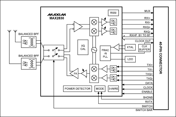
Figure 2. Block diagram of the WLAN reference design.
Power Consumption SummaryOperating conditions: VCC = 2.85V; VBAT = 3.3V; fRF = 2.437GHz; RXTX and active-low SHDN set according to operating mode; active-low CS = high; SCLK = DIN = low; transmitter and receiver in maximum gain. There were no input signals at RF inputs. Baseband outputs are open. 100mVRMS differential, 54Mbps IEEE 802.11g OFDM signals were applied to I and Q baseband inputs of transmitter in transmit mode.
| Parameter |
Test Conditions |
Meas. |
Unit |
| Supply Current |
Shutdown |
|
µA |
| Standby; PLL + VCO + LO generator |
28 |
mA |
| Rx active |
58 |
mA |
| Tx active (most linear mode) at 3.3V for PA VCC, POUT = 15.7dBm |
295 |
mA |
Receive SummaryOperating conditions: VCC = 2.85V; TA = +25°C; fRF = 2.437GHz; fBB = 4MHz; Rx VOUT = 112mVRMS; fREF = 40MHz; active-low SHDN = high; RXTX = low; active-low CS = high; SCLK = DIN = low.
| Parameter |
Test Condition |
Meas. |
Unit |
| Frequency Range |
|
2.4 to 2.5 |
GHz |
| Total Voltage Gain |
|
94 |
dB |
| RF Gain Steps |
Relative max gain (B7:B6 = 11) |
B7:B6 = 10 |
-16 |
dB |
| B7:B6 = 0X |
-33 |
| BB Gain Range |
Ratio of max to min gain |
61 |
dB |
| DSB NF |
LNA input referred, based on 10kHz to 8.6MHz integrated noise at I/Q baseband output. |
1. B7:B6 = 11, voltage gain = 90dB |
6.0 |
dB |
| 2. B7:B6 = 11, voltage gain = 62dB |
6.4 |
| 3. B7:B6 = 11, voltage gain = 48dB |
7.0 |
| I/Q Phase Error near DC |
Max gain |
< ±1 |
deg |
| IQ Gain Imbalance |
Max gain |
< 0.1 |
dB |
| Rx Sensitivity |
EVM < 9% |
Measured at J1 |
-73.6 |
dBm |
| Measured at J2 |
-72.6 |
| EVM |
PIN = -65dBm |
4.2 |
% |
| PIN = -40dBm |
2.2 |
| PIN = -10dBm |
3.0 |
Transmit SummaryOperating conditions: VCC = 2.85V; VBAT = 3.3V; TA = +25°C; fRF = 2.437GHz; fREF = 40MHz; active-low SHDN = high; RXTX = high; active-low CS = high; SCLK = DIN = low; 100mVRMS, 54Mbps 802.11g OFDM signal applied to I and Q baseband inputs of transmitter.
| Parameter |
Test Condition |
Meas. |
Unit |
| Frequency Range |
|
2.4 to 2.5 |
GHz |
| Transmit Power |
For EVM = 5.6%; meets the ACPR spec |
15.7 |
dBm/16MHz |
| Transmit EVM |
POUT = +15.7dBm |
5.4% |
|
| Adjacent Channel Power Ratio (for 54Mbps OFDM Signal) |
At 11MHz offset over 100kHz RBW |
See Figure 3 |
dBc |
| At 20MHz offset over 100kHz RBW |
| At 30MHz offset over 100kHz RBW | | |
| Operating Characteristics |
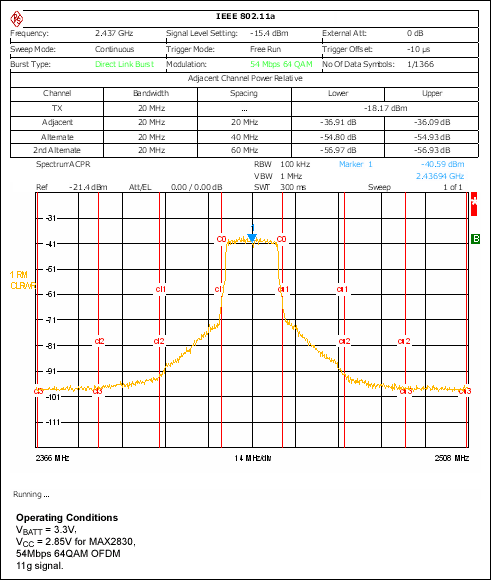 Figure 3. ACPR performance at Tx power = 15.7dBm, EVM < 5.6%.
 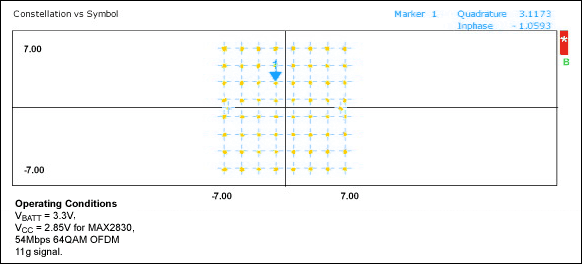 Figure 4. Rx I/Q constellation diagram at RF input = -40dBm, 54Mbps 64QAM, EVM = 2.2%. Figure 5. Rx I/Q constellation diagram at PIN = -65dBm, 54Mbps 64QAM. The EVM is only 4.2%, which is better than the 9% requirement for sensitivity.
This reference design is suitable for the full range of 802.11g OFDM data rates (6, 9, 12, 18, 24, 36, 48, and 54Mbps) and 802.11b QPSK data rates (1, 2, 5.5, and 11Mbps) at corresponding sensitivity levels. Using the MAX2830 chipset eliminates the need for external SAW filters, a RF switch, and a PA. Only a RF filter, RF balun, and a small number of passive components are required to form a complete 11b/g WLAN RF front-end solution that delivers high performance in a small
PCB form-factor.
IEEE is a registered service mark of the Institute of Electrical and Electronics Engineers.


 关注微信
关注微信