ADP1650是
ADI 公司的集成了
I2C兼容接口的1.5A
LED闪光
驱动器.器件集成了1.5MHz或3.0MHz同步电感升压
转换器,I2C兼容
接口和1500mA
电流源.火炬模式
电流高达200mA,效率大于90%(峰值),主要用在照相
手机和
智能手机以及
数码相机,摄像机和PDA.本文介绍了ADP1650主要特性,应用电路以及ADP1650 评估板套件主要特性,详细电路图和材料清单.
1.5 A LED Flash Driver with I2C-Compa
tible Interface
The ADP1650 is a very compact, highly eff
icient, single whi
te LED flash driver f
or high resolution camera phones that improves
picture and video quality in low light environments. The device integrates a prog
rammable 1.5 MHz or 3.0 MHz synchronous inductive boost converter, an I2C-compatible interface, and a 1500 mA current source. The high switching frequency enables the use of a tiny, 1 mm high, low cost, 1 μH power inductor, and the current source permits LED cathode grounding for thermally enhanced, low EMI, and compact layouts.
The LED driver
maximizes efficiency over the entire battery voltage range to maximize the input-power-to-LED-power conversion and minimize battery current draw during flash events. A programmable
dc battery current limit safely maximizes LED current for all LED VF and battery voltage conditions.
Two independent TxMASK inputs permit the flash LED current and battery current to reduce quickly during a power amplifier current bu
rst. The I2C-compatible interf
ace enables the pro-grammability of timers, currents, and status bit readback for operation monitoring and safety control.
The ADP1650 comes in a compact 12-ball, 0.5 mm pitch package and operates within specification over the full −40℃ to +125℃ junction temperature range.
ADP1650主要特性: Ultracompact solution
Small, 2 mm × 1.5 mm, 12-ball WLCSP package
Smallest footprint, 1 mm height, 1 μH power inductor
LED current source for local LED grounding
Simplified routing to/from LED
Improved LED thermals
Synchronous 3 MHz PWM boost converter, no external
diode High efficiency: 90% peak
Reduces high levels of input battery current during flash
Limits battery current drain in torch mode
I2C programmable
Currents up to 1500 mA in flash mode for one LED with 7% accuracy over all conditions
Currents up to 200 mA in torch mode
Programmable dc battery current limit (4 settings)
Programmable flash timer up to 1600 ms
Low VBAT mode to reduce LED current automatically
4-bit
ADC for LED VF, die/LED temperature readback
Control
I2C-compatible control registers
External STROBE and torch input pins
2 transmitter mask (TxMASK) inputs
Safety
Thermal overload protection
Inductor fault detection
LED short-/open-circuit protection
ADP1650应用: Camera-enabled cellular phones and smart phones
Digital still cameras, camcorders, and PDAs
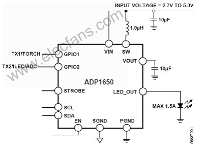
图1.ADP1650功能方框图
ADP1650 评估板
The evaluation system is composed of a motherboard, daughter- board and LED
sub-board. The motherboard provides the I2C signals from the PC
USB port and generates the I/O voltages and digital high and low signals for the daughterboard. For over-temperature measurement, the daughterboard
can either be plugged directly into the motherboard or connected to the motherboard via a ribbon cable.
The motherboard features a 3.3 V regulator and 2.8 V/1.8 V regulators for VDDIO. The daughterboard cont
ains jumpers and test points for easy evaluation of the flash driver IC.
The ADP1650-EVALZ kit includes:
Cables: power (red/black), USB, 2× current measurements
Samples: five ADP1650 devices, two FDSD3012 inductors
LED boards: OSRAM LUWF65N, LumiLEDs PWF-4
图2.ADP1650 评估板外形图

图3.ADP1650 评估板
主板电路图
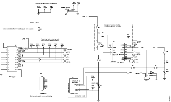
图4.ADP1650 评估板子板电路图
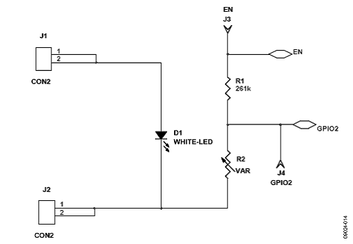
图5.ADP1650 LED插板电路图

图6.ADP1650- EVALZ电路图
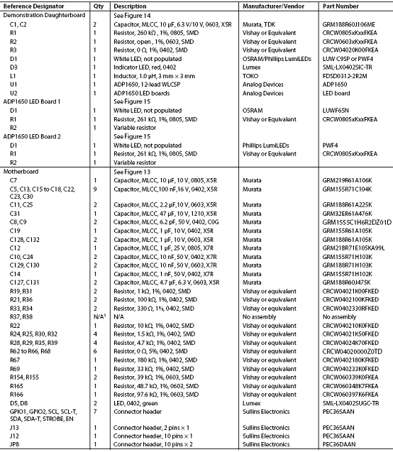
评估板材料清单(BOM):


 关注微信
关注微信