时间:2019-05-01 16:50
人气:
作者:admin
ST公司的BlueNRG-2是蓝牙标准兼容的非常低功耗蓝牙低功耗(BLE)单模式系统芯片(SoC),集成了256KB可编程闪存,24KB静态RAM存储器和SPI,UART,I2C标准通信接口,以及多功能计时器,RTC和DMA控制器,线性稳压器和DC/DC降压控制器,工作电压1.7V-3.6V,工作温度-40 °C到105 °C,主要用在手表,健美,健康和运动设备,消费类医疗设备,遥控,家庭和工业自动化,生活协助,手机外设,照明和PC外设。本文介绍了BlueNRG-2主要特性,架构图和总线架构图,时钟树和应用电路,以及BlueNRG-1/ BlueNRG-2开发板主要特性,电路图和材料清单。
The BlueNRG-2 is a very low power Bluetooth low energy (BLE) single-mode system-on-chip, compliant withBluetooth specifications.
The BlueNRG-2 extends the features of award-winning BlueNRG network processor, enabling the usage of theembedded Cortex M0 to run the user application code.
The BlueNRG-2 includes 256 kB of programming Flash memory, 24 kB of static RAM memory with retention (two12 kB banks) and SPI, UART, I²C standard communication interface peripherals. It also features multifunctiontimers, watchdog, RTC and DMA controller.
An ADC is available to interface with analog sensors, and to read the measurement of the integrated batteryvoltage sensor. A digital filter is available to process a PDM stream.
The BlueNRG-2 offers the same excellent RF performance of the BlueNRG radio, and the integrated highefficiency DC-DC converter keeps the same ultra-low power characteristics, but the BlueNRG-2 improves theBlueNRG sleep mode current consumption allowing a further increase in the battery lifetime of the applications.
BlueNRG-2主要特性:
• Bluetooth low energy single mode system-on-chip compliant with Bluetooth 5.0specifications:
– master, slave and multiple simultaneous roles
– LE data packet length extension
• Operating supply voltage: from 1.7 to 3.6 V
• Integrated linear regulator and DC-DC step-down converter
• Operating temperature range: -40 °C to 105 °C
• High performance, ultra-low power Cortex-M0 32-bit based architecture core
• Programmable 256 kB Flash
• 24 kB RAM with retention (two 12 kB banks)
• 1 x UART interface
• 1 x SPI interface
• 2 x I²C interface
• 14, 15 or 26 GPIOs
• 2 x multifunction timer
• 10-bit ADC
• Watchdog and RTC
• DMA controller
• PDM stream processor
• 16 or 32 MHz crystal oscillator
• 32 kHz crystal oscillator
• 32 kHz ring oscillator
• Battery voltage and temperature sensors
• Up to +8 dBm available output power (at antenna connector)
• Excellent RF link budget (up to 96 dB)
• Accurate RSSI to allow power control
• 8.3 mA TX current (@ -2 dBm, 3.0 V)
• Down to 1 μA current consumption with active BLE stack (sleep mode)
• ST companion integrated balun/filter chips are available
• Average advertisement current consumption 15.34 μA (advertisement interval1000 ms) – 1 year, 8 months, 19 days with 230 mAh battery (CR2032)
• Average connection current consumption 7.059 μA (connection interval 1000ms) – 3 years, 10 months, 12 days with 230 mAh battery (CR2032)
• Suitable for building applications compliant with the following radio frequencyregulations: ETSI EN 300 328, EN 300 440, FCC CFR47 part 15, ARIB STDT66
• Pre-programmed bootloader via UART
• QFN32, QFN48 and WCSP34 package options
BlueNRG-2应用:
• Watches
• Fitness, wellness and sports
• Consumer medical
• Security/proximity
• Remote control
• Home and industrial automation
• Assisted living
• Mobile phone peripherals
• Lighting
• PC peripherals
The BlueNRG-2 integrates:
• ARM Cortex-M0 core
• Interrupts management
• 256 kB Flash memory
• 24 kB of RAM with two retention options (12 kB or 24 kB)
• Power management
• Clocks
• Bluetooth low energy radio
• Random number generator (RNG) (reserved for Bluetooth low energy protocol stack, but user applicationscan read it)
• Public key cryptography (PKA) (reserved for Bluetooth low energy protocol stack)
• Peripherals:
– SPI interface
– UART interface
– I²C bus interface
– GPIO
– Multifunction timer
– DMA controller
– Watchdog
– RTC
– ADC with battery voltage sensor and temperature sensor
– PDM stream processor
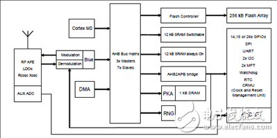
图1.BlueNRG-2架构图
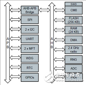
图2.BlueNRG-2总线架构图
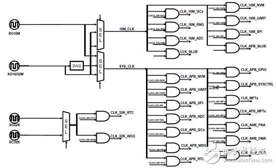
图3.BlueNRG-2时钟树
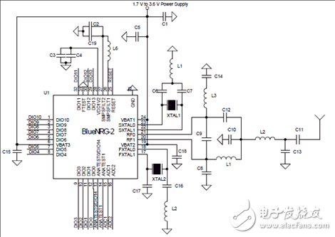
图4.BlueNRG-2应用电路:有源DC/DC转换器,QFN32封装
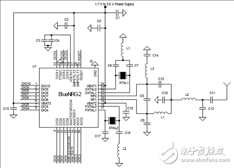
图5.BlueNRG-2应用电路:非有源DC/DC转换器,QFN32封装
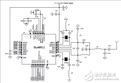
图6.BlueNRG-2应用电路:有源DC/DC转换器,WCSP34封装
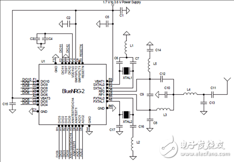
图7.BlueNRG-2应用电路:非有源DC/DC转换器,WCSP34封装
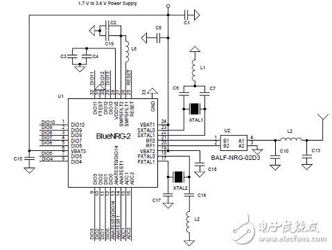
图8.BlueNRG-2应用电路:有源DC/DC转换器,QFN32封装带BALF-NRG-02D3平衡/平衡变换器
BlueNRG-1/ BlueNRG-2开发板

 关注微信
关注微信