时间:2017-11-25 13:50
人气:
作者:admin
NS 公司的ADC16V130是LVDS输出的16位130MSPS高性能ADC,双电源1.8V和3.0V工作,16位分辨率,取样速率130MSPS,满功率带宽1.4GHz,160-MHz的SNR为76.7dB, SFDR为90.6dBFS,主要应用在高IF取样接收器,多载波基站接收器,测试测量设备,通信基础设备,数据采集和手提仪表等.本文介绍了ADC16V130主要特性,方框图,低频和高频变压器驱动电路以及SP16130CH4RB低IF接收器参考设计主要特性,详细电路图和材料清单(BOM).
ADC16V130: 16-Bit, 130 MSPS A/D Converter with LVDS Outputs
The ADC16V130 is a monolithic high performance CMOS analog-to-digital converter capable of converting analog input signals into 16-bit digital words at rates up to 130 Mega Samples Per Second (MSPS). This converter uses a differential, pipelined architecture with digital error correction and an onchip sample-and-hold circuit to minimize power consumption and external component count while providing excellent dynamic performance. Automatic power-up calibration enables excellent dynamic performance and reduces part-to-part variation, and the ADC16V130 could be re-calibrated at any time by asserting and then de-asserting power-down. An integrated low noise and stable voltage reference and differential reference buffer amplifier easies board level design. On-chip duty cycle stabilizer with low additive jitter allows wide duty cycle range of input clock without compromising its dynamic performance. A unique sample-and-hold stage yields a fullpower bandwidth of 1.4 GHz. The digital data is provided via full data rate LVDS outputs – making possible the 64-pin, 9mm x 9mm LLP package. The ADC16V130 operates on dual power supplies +1.8V and +3.0V with a power-down feature to reduce the power consumption to very low levels while allowing fast recovery to full operation.
ADC16V130主要特性:
■ Dual Supplies: 1.8V and 3.0V operation
■ On chip automatic calibration during power-up
■ Low power consumption
■ Multi-level multi-function pins for CLK/DF and PD
■ Power-down and sleep modes
■ On chip precision reference and sample-and-hold circuit
■ On chip low jitter duty-cycle stabilizer
■ Full data rate LVDS output port
■ 64-pin LLP package (9x9x0.8, 0.5mm pin-pitch)
ADC16V130主要指标:
■ Resolution 16 Bits
■ Conversion Rate 130 MSPS
■ SNR
(fIN = 10MHz)
(fIN = 70MHz)
(fIN = 160MHz)
78.5 dBFS (typ)
77.8 dBFS (typ)
76.7 dBFS (typ)
■ SFDR
(fIN = 10 MHz)
(fIN = 70MHz)
(fIN = 160MHz)
95.5 dBFS (typ)
92.0 dBFS (typ)
90.6 dBFS (typ)
■ Full Power Bandwidth 1.4 GHz (typ)
■ Power Consumption
Core
LVDS Driver
Total
650 mW (typ)
105 mW (typ)
755 mW (typ)
■ Operating Temperature Range -40°C ~ 85°C
ADC16V130应用:
■ High IF Sampling Receivers
■ Multi-carrier Base Station Receivers GSM/EDGE, CDMA2000, UMTS, LTE and WiMax
■ Test and Measurement Equipment
■ Communications Instrumentation
■ Data Acquisition
■ Portable Instrumentation
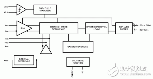
图1.ADC16V130方框图
图2. ADC16V130低频输入变压器驱动电路
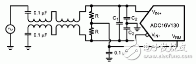
图3. ADC16V130高频输入变压器驱动电路
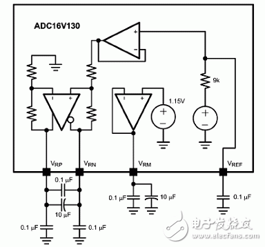
图4. ADC16V130内部基准和去耦电路
上一篇:单芯片无线MCU性能分析详解
下一篇:RF电路和数字电路设计中常见问题


 关注微信
关注微信