Abstract: This appl
ica
tion no
te cont
ains inf
ormation necessary to interface the Motorola MC68360 processor to the DS2141Q or the DS2143Q Dallas Semiconductor T1 or E1 f
rame
rs. The application note covers interfacing both the
address and data processor bus and the communications serial bus. Interfacing the processor bus of the MC68360 to the DS2141Q or DS2143Q is straigh
tforward and map
ping of address and data lines is shown in the diagram. Depending on the application, it may be necessary to add external
logic to latch the address and data pins isolate other peripheral on the processor bus. The MC68360 contains a communications processor module that has four serial communications controllers and two serial management controllers. Any of these six ports
can be mapped into the MC68360 time slot assigner to provide two time division multiplexed buses for the DS2141Q or DS2143Q. The communication serial bus pin and clock names and descriptions for the MC68360 are shown in the diagram for easy reference. The example circuit diagram is of a loop timed application used in customer premises equipment where the recovered clock is used as the transmit clock. The goal of the application note is to give the designer enough information to complete a b
asic schematic diagram.
Interconnections between the DS21Q41 or DS21Q43 and the Motorola MC68MH360 (QUICC32) are shown in Figure 1. The MC68MH360 can be configured as an HDLC controller implementing protocols such as LAPD for both DS0 channel and the FDL or E1 Sa bits. Any combination of the QUICC32's SCCs and SMCs can be processed through an internal time slot assigner onto one or two Time Division Multiplex channels, TDM A and TDM B. In the configuration shown, TDM channel A is used for timeslots 0-23 (T1) or 0-31 (E1) and TDM channel B is used for the FDL (T1), or Sa bits (E1). See the MC68MH360 Quad Integrated Communications Controller user's manual for complete details.
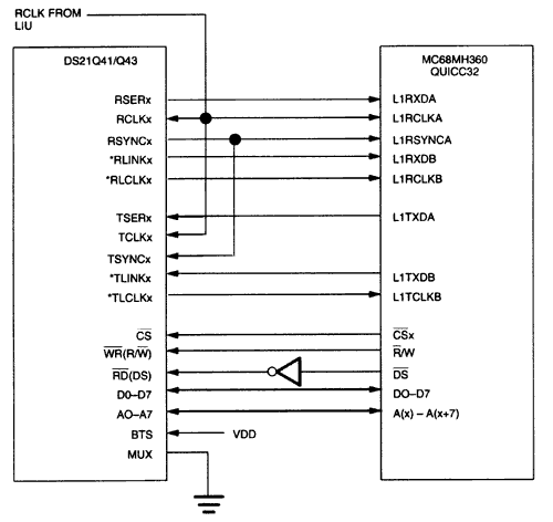
Figure 1. Quad framer - QUICC32 interconnections.
*HDLC on the FDL can be implemented either by TDM CHANNEL B or via the port by the host processor (
CPU32 internal to the QUICC32).
DS21Q41, DS21Q43 Notes:
- Other signals affecting operation of device are not shown.
- Example circuit has RSYNC in output mode.
MC68360 Notes:
- Other signals affecting operation of device are not shown.
- Use SI mode register t
- Set up transmit and receive frame sync delays (0-3 clocks) to mask the F-Bit in T1 applications. RFSDA = 1 for DS21Q41, 0 for DS21Q43.
- Set clock edges for transmit on rising edge and receive on falling edge. CEA = CEB = 0.
- In the above example, TDM channel A has a common transmit/receive clock and sync. CTRA = 1.
- Use the TIMESLOT ASSIGNER to ignore Timeslot 0 for the DS21Q43.


 关注微信
关注微信