时间:2009-04-22 10:14
人气:
作者:admin
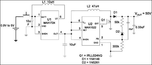
Figure 1. These two boost converters in cascade can produce +50V from a single-cell input.
No single IC at this time is capable of converting a single-cell output to 50V, but the 2-stage step-up converter of Figure 1 handles the task. Because the fixed-output, low-power boost converter (U1) accepts voltages in the range 0.9V to 5V, the circuit’s power source can include batteries of various chemistries and cell counts—such as one Li-ion cell, one to three alkaline cells, or one to four NiMH cells.
U1 provides a fixed 5V output that is stepped up by a low-cost boost controller (U2) to +50V. For input voltages above 1.8V, the circuit generates +50V at load currents above 6mA. For a single alkaline or NiMH cell, it generates +50V with more than 1mA of load current. (Both ICs come in small SOT23 packages.)
You should choose a MOSFET with breakdown voltage above 55V and a rated current above 0.8A. A 1N4148 or other low-cost silicon diode serves for the rectifier. The forward voltage drop across that diode is negligible in a +50V system. Because, moreover, the load current is low (single-digit milliampere range), the diode’s power dissipation is minuscule. A 47V zener diode (D2) in conjunction with 300k in the feedback loop lowers the circuit’s supply current. Quiescent supply current declines as you raise the input voltage (Figure 2).
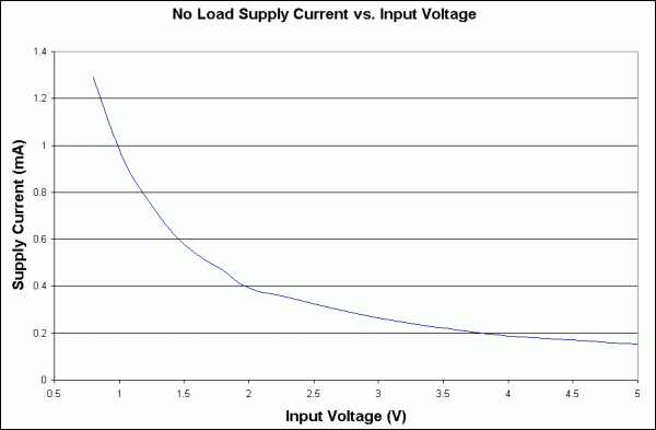
Figure 2. Quiescent supply current for the Figure 1 circuit declines as the input voltage increases.
Efficiency for the circuit is the product of U1 efficiency and U2 efficiency, and varies with input voltage and load current (Figure 3). You might think that efficiency can be improved by connecting one end of L2 directly to the single-cell input, but not so. Instead, to accommodate the variation of input to output voltage, you must choose an inductor that achieves the highest efficiency over the full range of input voltages. With L2 connected to the input, the best efficiency is obtained for an L2 value of 6.1µH. With U1 and U2 cascaded as shown, on the other hand, the highest efficiency occurs for an L2 value of 47µH. Efficiencies for the two configurations are actually similar, with the cascaded configuration only 1% higher. The cascaded version also produces a smaller and more predictable output ripple over the full range of input voltages.
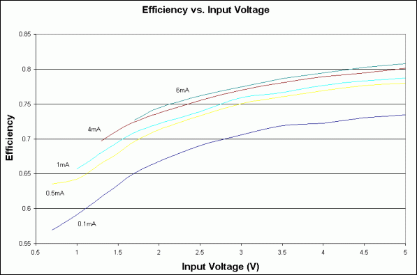
Figure 3. Efficiency for the Figure 1 circuit varies with load current and input voltage as shown.
This design idea (#562) appeared in the 10/18/04 issue of the Planet Analog supplement in EE Times.
下一篇:天津手机展提供全球性采购配套机会

 关注微信
关注微信