Reference Design of a 1-Wire Bidirectional Voltage-Level Translator for 1.8V to 5V
Abstract: Designers need open-drain logic to run at 1.8V at the 1-Wire master IO. Most 1-Wire slave devices cannot run at 1.8V. This application note presents an RD (reference design) of a circuit that translates from a 1.8V 1-Wire master to a 5V 1-Wire slave device. The RD is used for driving typical 1-Wire slave devices. The MAX3394E voltage-level translator is featured in the design.
Introduction
Devices such as
FPGAs, microprocessors, the DS2482-100, and DS2480B are examples of 1-Wire master devices. The 1-Wire/iButton® slave devices are manufactured by
Maxim and comprise an extensive family of parts that typically operate from 2.8V to 5.25V. The 1-Wire masters and slave devices have tr
aditionally been 5V open-drain logic in the past.
Today designers need open-drain logic to run at 1.8V at the 1-Wire master IO. While most 1-Wire slave devices can run safely at 5V, most of those same devices cannot run at 1.8V. A bidirectional voltage-level translator circuit is needed to overcome this limitation. This RD (reference design) features the Maxim® MAX3394E, which is a bidirectional voltage-level translator for these applications.
Voltage-Level Translator
The MAX3394E is a dual-level translator av
ailable in an 8-
pin, 3mm x 3mm TDFN package. It is ideal for driving high-capacitive lo
ads, thanks to its internal slew-rate enhancement circuitry. 1-Wire slave devices often have capacitive loading greater than 500pF. The MAX3394E's VCC I/O pins are protected to ±15kV HBM (Human Body Model), which protects the 1-Wire master. The 1-Wire bus architectures often interface to the external world, making HBM essential. However, it is
recommended that a DS9503P be added as
ESD protection for the pullup resistor (R3), the optional strong pullup circuitry, and the 1-Wire slave device.
Application Circuit
The circuit in Figure 1 shows the MAX3394E used to pe
rform bidirectional 1.8V to 5V voltage-level translation in an open-drain system.
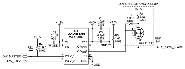
Figure 1. Schematic of 1-Wire bidirectional voltage level translation from 1.8V to 5V. Note that the pins I/O VL and I/O VCC have a typical 10kΩ internal pullup.
The BOM (bill of materials) for this reference design is given in Table 1.
Table 1. Bill of Materials
| Item |
Quantity |
Reference |
Part |
Manufacturer |
Part Number |
| 1 |
1 |
C1 |
1.0µF 0402 |
Panasonic |
ECJ-0EB0J105M |
| 2 |
2 |
C2, C3 |
0.1µF 0201 |
Panasonic |
ECJ-ZEB0J104K |
| 3 |
1 |
Q1 |
BSS84-7-F |
Diodes, Inc/Zetex |
BSS84-7-F |
| 4 |
1 |
R1 |
33Ω 0201 |
Panasonic |
ERJ-1GEJ330C |
| 5 |
1 |
R2 |
10kΩ 0402 |
Panasonic |
ERJ-2RKF1002X |
| 6 |
1 |
R3 |
1kΩ 0402 |
Panasonic |
ERJ-2RKF1001X |
| 7 |
1 |
R4 |
2.2kΩ 0402 |
Panasonic |
ERJ-2RKF2201X |
| 8 |
2 |
CH1, CH2 |
TEST POINT |
N/A |
N/A |
| 9 |
1 |
U1 |
MAX3394E |
Maxim |
MAX3394EETA+ |
Waveform Measurements/Test Results
The test results in Figures 2 through 5 were generated from the board built for evaluating the circuit.
Setup:
- VL = 1.8V
- VCC = 5.0V
- CH1: 1-Wire master (OW_MASTER)
- CH2: DS1920 (OW_SLAVE)
- OW_SLAVE wire length: 2.4m, max.
- Test results did not include the optional strong pullup circuitry in Figure 1.
- Room temperature measurements only
Figure 2. The scope plot of a 1-Wire Reset shows the performance of the MAX3394E with presence pulse amplitude of no more than 250mV, lower than a typical 1-Wire master VIL maximum of 0.4V.
Figure 3. The scope plot of a 1-Wire Write, one timeslot with a clean tLOW1 < 15µs.
Figure 4. The scope plot of a 1-Wire Write, zero timeslot with 60µs < tLOW0 < 120µs.
Figure 5. The scope plot of a 1-Wire Read, zero timeslot with an
active 1-Wire slave open-drain return and lower than a typical 1-Wire master VIL maximum of 0.4V.
Conclusion
This RD for 1.8V to 5V 1-Wire bidirectional logic-level translation drives typical 1-Wire slave devices. The design was built and then tested. The circuit schematic, BOM, and typical waveforms have been presented.


 关注微信
关注微信