时间:2017-12-27 06:21
人气:
作者:admin
Outline
1. Charge-trap eNVMs at Cypress
2. SONOS
–Introduction
–Key Macro Specs
–High Reliability
3. eCT
–Introduction
–Key Macro Specs
–High Reliability
4. Embedded NVM Solutions for Various Applications
Charge-trap eNVMs at Cypress
Cypress develops, uses and licenses two embedded NVM technologies
SONOS and eCT,both are charge-trap non-volatile memories.
SONOS: Silicon Oxide Nitride Oxide Silicon
Originally developed at Sandia National Lab, CY acquired it in 1998.
Available at 0.35µm, 0.13µm, 95nm, 65nm, 55nm, 40nm and 28nm process nodes.
Shipped>1,200,000 wafers from foundry partners HHGrace, HLMC and UMC.
Low cost, Lowpower, suitable for IoT, consumer, industrial, and automotive grade2/3 applications.
eCT : embedded Charge Trap
Former Spansion’s eNVM technology for automotive MCUs.
Based on 6 generations of Mirror Bit technologies.
In production (MCUs) at 40 nm node at UMC.
Automotive Grade-1 qualified.
Key Features
SONOS Introduction
Silicon Oxide Nitride Oxide Silicon
A planar, scalable MOS transistor with an ONO stack as the gate dielectric.
Store captured charges in discrete traps in the nitride (N) layer through FN tunneling.
Low Cost, Low Power, High Security
Lowest cost: Only 3~5 extra masks added into standard CMOS process.

Lowest power: 7.5V program/erase voltage, low-current FN/FN program/erase operations.
High Security: Resistant to decode by de-processing.
Ideal solution for consumer, industrial and especially IoT SoCs.
> MCU, Smart Card,EEPROM, FPGA, NOR Flash, etc.
Key SONOS Macro Specs

55 nm SONOS Macro Power Consumption
Balanced power consumption and performance (20ns Taa) for many applications
−Three power-saving modes: hibernate, sleep and standby.
−Low power read and program/erase operations to minimize active power.
−Low power read operation with Vdd=1.08 V to1.32 V.

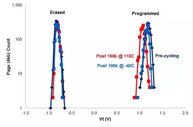
500hrs 225°C Yield w/ 50K Pre-cycling at 85 °C (55nm)
*All dies pass reading on full 8Mb after 500hrs 225°C bake
High Reliability
55-nm SONOS Macro Reliability
Endurance passes 500K cycles at 85°C w/o ECC. Vt window > 1.2V after 500K cycling.
Retention passes Automotive Grade-2 AEC Q100 requirement.
> Vt window > 0.6 V after 500 hrs bake @ 225C with 50K pre-cycling.


>滑动查看下一张图片<
40-nm SONOS Macro Reliability
Endurance passes 500K cycles at 85°C w/o ECC. Vt window > 1.2V after 500K cycling.
Retention passes Automotive Grade-2 AEC Q100 requirement
>Vt window > 0.6 V after 500 hrs bake @ 225C with 50K pre-cycling.

>滑动查看下一张图片<
28-nm SONOS Macro Reliability
Endurance passes 10K cycles at 125°C, Vt window >1.4 V after cycling.
Retention passes accelerated 48-hour bake at 250°C with > 0.7 V window left.


>滑动查看下一张图片<
55nm SONOS in Production Press Release
Customers NPI Status @ HLMC 55nm SONOS
Engaged > 15 customers.
7 Customers signed contract to use
3 in mass production
> 1,000 wafers started per month

SONOS eNVM Technology Availability
SONOS eNVM is scalable and proven in volume production on many nodes.

eCT Introduction
embedded Charge Trap
Based on charge-trap technology proven in six generations of MirrorBit® NOR Flash memory
Ideal solution for high-performance automotive MCUs
Fast 8 ns random access time from -40°C to 150°C junction temperature and 30 ms word programming speed
Smallest eNVM bit cell in the industry, 0.053 sq. µm, at 40 nm node
Automotive Grade-1 reliability
Applications
Hybrid and electric vehicle motor control, instrument clusters, body control modules and HVAC
In volume production on UMC 40LP process flow
Key eCT Macro Specs

eCTReliability:
Automotive Qualification Data
Passed accelerated stress tests for Automotive Grade-1 per AEC-Q100 standard

40nm eCT in Production Press Release

Embedded NVM Solutions for Various Applications
Conclusion
Cypress develops and licenses charge-trap NVM technologies and Flash macro IP
Charge-trap NVMs serve in a wide range ofembedded applications
−SONOS: Consumer, Industrial SoCs
−eCT: high-performance automotive MCUs,Automotive Grade-1 reliability
Technologies are scalable to advanced nodes
−SONOS in mass production from 0.35um to 55nm, engineering samples available on 40uLP & 28HLP
−eCT is in volume production on UMC 40LP process
Low power for IoT: 0.9 V (40nm) or 1.2V(55nm) power supply, low-current operation, power-saving modes
Cost-effective: 3~5 (SONOS) or 8 (eCT)extra masks beyond the standard CMOS.


 关注微信
关注微信