Abstract: This audio bridge-
tied lo
ad (BTL) amplifier appl
ication no
te describes a unique architecture that minimizes the differential output dist
ortion and noise (THD+N).
免费注册参加在线研讨会,学习如何分析、测量并最终解决音频系统的设计问题 (English only) 。
| |
Low-voltage systems driving lou
dspeake
rs often employ a bridged-amplifier configuration that effectively doubles the voltage swing at the tran
sducer (speaker). In a typical bridge-amplifier circuit (Figure 1), an
AC-coupled inverting stage with g
ain drives one side of the speaker. It also drives a second unity-gain inverting amplifier, which drives the other side of the speaker.
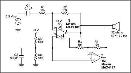
Figure 1. This conventional bridged amplifier features two amplifiers in tandem.
Bridged amplifiers usually incorporate a matched pair of amplifiers, but the first amplifier dominates overall pe
rformance because its output noise and distortion are replicated in the second amplifier. You
can eliminate this drawback by placing the two amplifiers in a non-cascaded configuration, in which one is inverting and the other in non-inverting (Figure 2). Both amplify the same input signal, so neither one reproduces noise, distortion, or clip
ping introduced by the other.
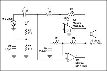
Figure 2. This circuit optimizes the Figure 1 configuration by apportioning gain between the two amplifiers.
As a key improvement in Figure 2,
DC bias for the non-inverting circuit is derived from the inverting amplifier's source resistor. (Bias is required because the input is AC coupled). Using the other amplifier's source resistor as a bias source lowers the component count and eliminates signal injection into the high-imp
edance bias source (VCC/2, applied to the top amplifier's non-inverting input).
Another advantage in Figure 2 is the elimination of DC gain in the non-inverting amplifier. For the circuit shown, C2 sets the -3dB point at half the input cutoff frequency, and R1/C1 sets the input highpass cutoff frequency at 100Hz.
A
similar version of this article appeared in the November 19, 2001 issue of Electronic Design magazine.


 关注微信
关注微信