Abstr
act:
Analog switches are commonly used in audio sys
tems to switch low-level inputs
or adjust audio filter characteris
tics. Selecting the proper analog switch
can help optimize the total harmon
ic distortion (THD) of a system within the designer's cost budget.
免费注册参加在线研讨会,学习如何分析、测量并最终解决音频系统的设计问题 (English only) 。
| |
Analog switches are commonly used in audio systems to switch low-level inputs or adjust audio filter characteristics. Selecting the proper analog switch can help optimize the total harmonic distortion (THD) of a system within the designer's cost budget.
THD specification plays a critical role in determining the quality or fidelity of audio signals passing through or generated by audio systems. Thus, when designing audio systems, importance must be placed on selecting the proper components and board layout to minimize THD.
When passing a signal through a switch, the switch must not degrade signal integrity or introduce any new information onto the desired output signal. Any change in waveform is considered to be distortion and is obviously undesirable and also impossible to avoid, and thus must be minimized.
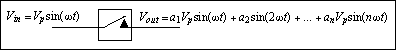
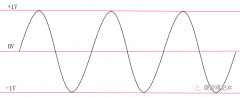
Figure 1.
THD is defined as the square root of the ratio of the sum of all of the squared second, third, and higher harmonics to the magnitude of the fundamental harmonic.
Selecting an analog switch with a minimum THD requires one with low on-resistance (RON) and consequently low on-resistance flatness (
RFLAT(ON)). Some analog-switch data sheets neglect to specify flatness, but it can be assumed to be approximately 10% of the on-resistance. Flatness is defined as the difference between the
maximum and minimum values of on-resistance as measured over the specified analog-signal range.
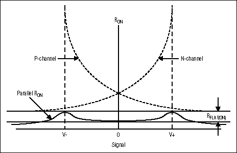
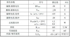
Figure 2. RFLAT(ON).
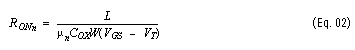
The on-resistance curves are determined by the length L, width W, electron and hole mobility (µn and µp, respectively), oxide capacitance COX, threshold voltage VT, and signal voltage VGS (VIN) of both
MOSFETs.
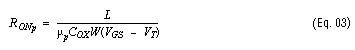
As illustrated above, the on-resistance for the PMOS and the NMOS are in parallel, resulting in resistance R, which is a non
linear function. The source of distortion arises from parallel PMOS and NMOS in series with constant load, causing a nonlinear attenuation of the signal passing through the switch. With multiple switches, THDs will add together. The following schematic shows this resistor-divider relationship of the switch and the load.
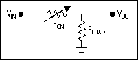
Figure 3.
In practical te
rms, maximum THD is determined by the following equation:
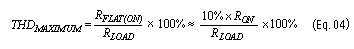
As observed in Figure 2, parallel RON, and therefore RFLAT(ON), can vary depending on the analog input signal, and maximum THD will occur at the greatest difference between the maximum and minimum values of the parallel RON. Therefore, an analog input signal operating about a point below the maximum value will experience a lower THD.
Three different switches are shown below along with their on-resistance and corresponding measured THD. A standard test load of 10 kilohms was used to obt
ain the plot.
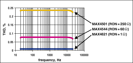
Figure 4. THD vs. frequency.
In audio systems, imp
edance loads of 1200, 600, 36, 32, 16, 8, 4, and 3 kilohms will be encountered, and, especially with very low impedances, on-resistance flatness (RFLAT(ON)) must be taken into consideration to minimize THD. Equation 4 will provide a starting point in selecting an analog switch if THD is the highest priority.


 关注微信
关注微信