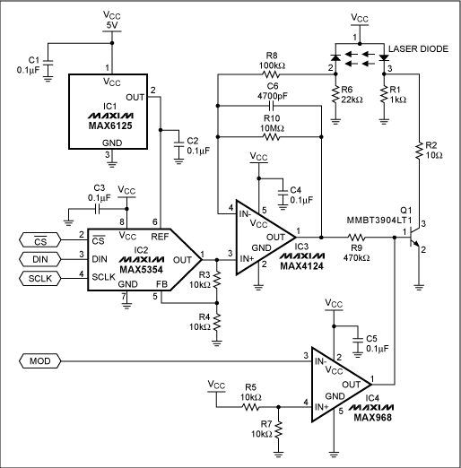
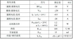
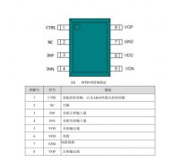
Abstract: The circuit in the figure below includes a 10-bit digital-to-
analog conver
ter (
DAC) with 3-wire serial input that operates and m
aintains a visible-light laser
diode at constant average op
tical output power. A separate digital input line (MOD) enables a comparator with open-drain output (
IC4) to implement digital communications by pulsing the laser-diode through Q1.
Many laser diodes include a photodiode that generates a current prop
ortional to the intensity (optical power) of the laser beam. Most of these photodiodes, however, have relatively slow response times and
cannot tr
ack the peak optical power of a typical modulated laser diode. Inste
ad, the driver circuits for these devices control the laser by monitoring a relative average optical power.
The circuit in the figure below includes a 10-bit digital-to-analog converter (DAC) with 3-wire serial input that operates and maintains a visible-light laser diode at constant average optical output power. A separate digital input line (MOD) enables a comparator with open-drain output (IC4) to implement digital communications by pulsing the laser-diode through Q1. Circuit components were chosen to minimize the layout are and cost.
For Larger Image
This circuit provides digital control of the modulation and power output of a visible-light laser diode.
Resistor R6 converts the photodiode current to a usable voltage, which is applied to the inverting input of a "leaky" integrator based on the high-speed op amp IC3. The integrator smoothes out variations in the modulation and prevents the feedback loop from trying to regulate the laser pulses. The integrator is made leaky (by R10) to ensure compensation of downward as well as upward variations in the average power.
Thus, the integrator creates an error signal and base drive for Q1 by monitoring the voltage ac
ross R6 and comparing it to the DAC's preset voltage. The DAC's reference voltage (from IC1) is 2.5V, but its output-voltage buffer has a gain of 2V/V, giving the DAC output an adjustment range of 0 to 5V. With its nominal base voltage set by the DAC output, Q1 controls the optical power by regulating current through the laser diode.
R9 provides isolation and helps to stabilize IC3 when the base of Q1 is being shorted and released by a signal from the MOD input. By maintaining a small laser-diode current during the "off" periods of digital modulation, R1 preempts another problem: Startup time for a laser diode increases tremendously if the forward current goes to zero. R1 ensures that the laser current is below the threshold for lasing, but high enough to allow an acceptable turn-on time for communication and modulation.
A
similar version of this article appeared in the March 23, 1998 issue of Electronic Design magazine.


 关注微信
关注微信