Abstract: Build a composite amplifier featuring high gain, wide bandwidth, good DC accuracy and low distortion by cascading a dual amplifier and adding phase compensation. You
can build a composite amplifier featuring high gain, wide bandwidth, and good DC accuracy by cascading the sections of a dual video amplifier and adding two appropriate phase-compensation components. In the example shown (
Figure 1) the op amp drives a 150Ω load and provides a closed-loop gain of 40dB. You can obtain 40dB by cascading two 20dB sections, but that arrangement allows signif
icant output distortion. (The video amplifie
rs normally opera
te at low gain while driving 75Ω or 150Ω loads.
The individual video amplifiers are unity-gain stable without external compensation, and have unity-gains bandwidth of 72MHz. They operate on ±5V supplies and consume about 350mW as a pair. Other typical specs include 2mV input offset, 100pA input bias currents, -72dB isolation between amplifiers, and differential phase and gain errors of 0.2° and 0.5%. The dual-amplifier chip comes in an 8-lead DIP.
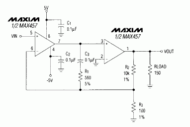 Figure 1. This composite amplifier, based on a dual video-amplifier IC, provides a 40dB gain and 10MHz bandwidth while driving a 150Ω load.Max457 pdf datasheet.
The approach taken in Figure 1 minimizes output distortion. The first amplifier, operating with no (DC) load, provides it's
maximum voltage gain of about 660V/V. The second amplifier, drivng a 150Ω load, has a voltage gain of about 65. Total open-loopgain for the composite amplifiers is thus 660×65, or about 92dB. In the absence of phase-compensation componenets R
1 and C
3, however, the circuit will oscillate.
With the 150Ω load, output swing is typically ±3.3V and
linearity (between -2V and 2V) is about ±0.5%. R
1 and C
3 adjust the -3dB frequency to 10MHz, giving a gain-bandwidth product of 1GHz. The amplifier provides a 2V output swing with only 3% peaking near the 10MHz rolloff frequency. For comparison, a BB3554 or AD3554 operating at 40dB with no phase compensation (for
maximum bandwidth) has a -3dB bandwidth of only 7MHz.
Table 1. Input and output voltages.
(Offset voltage not adjusted)
| VIN |
VOUT |
| +30.000mV |
+2.968V |
| +20.000mV |
+1.963V |
| +10.000mV |
+0.960V |
| 0.000mV |
-0.046V |
| -10.000mV |
-1.060V |
| -20.000mV |
-2.070V |
| -30.000mV |
-3.059V |
The table in Figure 1 gives DC pe
rformance for the closed-loop amplifier. Gain resistors R
2 and R
3 measured 99.78 and 9965Ω, giving a theoretical gain of R
2 + R
3 / R
3 = 1000.870V/V—which is very close to the value of 100.825 measured for range -2V to 2V.

 关注微信
关注微信