时间:2023-06-19 11:14
人气:
作者:admin
编者注:PCIE5.0已经开始在产品中应用,在下也参与了几个PCIE5.0相关的项目,有系统级的,也有元器件级别的,在设计中确实也存在一些挑战。比如在规范中也针对过孔设计做了说明。如下图所示为PCIE5.0金手指Pad的设计示意图。

本文是今年发布在DesignCon的文章,介绍了如何进行仿真和设计,以及过孔对系统的影响等等,最后结合仿真与测试,一并对比了前仿真、后仿真以及测量的结果,非常有参考意义,值得学习。


Conclusion
Extract Via EM models to a very high bandwidth:
o Since structures are small the extra simulation time from a denser FEM mesh is not a limiting factor. Yet the high stop frequency (80GHz) gave necessary extra resolution in the TDR response. This is important when comparing small differences between parameter values and deciding what effect if the adjustment of this parameter was trending in the right direction.
Use more than one figure of merit:
oAn eye diagram alone is not enough to determine which via design is best, particular for small changes in ISI that may be compensated by Rx equalization. Instead, the key figures of merit during optimization were Insertion Loss, Return Loss, TDR, NEXT & FEXT, giving a rounded view of the behavior of the via or Via Array. Often, picking an optimal design that is practical to build is a challenging endeavor, but having multiple FOMs gives the designer confidence in their choice. Likewise, the final system simulation with equalized eye diagrams provides the final decision on whether the design, and full channel passes the spec. In the duration of this work, some figures of merit such as ‘Signal Spectrum at the Tx’ and ‘Signal Spectrum at the Rx’ were thrown away, as deemed not useful.
What is worse? A lower via impedance due to excess capacitance, or a via that transitions between capacitive & inductive?
oThis is difficult to predict from viewing the TDR alone, but having several figures of merit to rely on verified that having a much lower impedance due to excess capacitance was clearly worse.
Laser Vias for highest speed:
o In all cases, the shortest via transitions were best if they can be practically applied.
Take care of NEXT / FEXT:
o System simulations demonstrated that sub optimal design combinations could lead to >12dB increase in both NEXT and FEXT at Nyquist. In all cases though, these values were still well below the rule of thumb (< 20dB).
Shared stitching vias in a Via Array?
o No. If you have space, it is best to provide separate stitching vias closest to the longest part of the via (Buried via in th is instance).
Reference Models:
o A critical piece of the system validation process is access to a standard specific PCIe Gen5 IBIS AMI Rx model with adaptive EQ.
编辑:黄飞
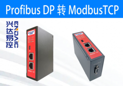
从profibusDP转ModbusTCP,一网打尽转换技巧!


 关注微信
关注微信