时间:2018-06-07 00:30
人气:
作者:admin
ADI公司的ADSP-BF70x Blackfin处理器系列采用双MAC 16位最新的处理引擎,正交RISC类微处理器指令集,在单指令架构中采用单指令多数据(SIMD)多媒体功能, Blackfin+核能工作高达400MHz,每周妻支持双16位或单32位MAC,其低功耗性能可应用在汽车电子,视频/图像分析,工业控制,马达控制,仪器仪表,电源控制和生物计量。本文介绍了ADSP-BF70x Blackfin处理器系列主要特性,框图和Blackfin+处理核框图,以及评估板ADSP-BF707 EZ-KIT Lite 主要特性,框图,电路图,材料清单和PCB布局设计图。
The ADSP-BF70x processor is a member of the Blackfin family of products. The Blackfin processor combines a dual- MAC 16-bit state-of-the-art signal processing engine, the advantages of a clean, orthogonal RISC-like microprocessor instruction set, and single-instruction, multiple-data (SIMD) multimedia capabilities into a single instruction-set architecture. New enhancements to the Blackfin+ core add 32-bit MAC and 16-bit complex MAC support, cache enhancements, branch prediction and other instruction set improvements—all while maintaining instruction set compatibility to previous Blackfin products. The processor offers performance up to 400 MHz, as well as low static power consumption. Produced with a low-power and low-voltage design methodology, they provide world-class power management and performance. By integrating a rich set of industry-leading system peripherals and memory (shown in Table 1), the Blackfin processor is the platform of choice for next-generation applications that require RISC-like programmability, multimedia support, and leading-edge signal processing in one integrated package. These applications span a wide array of markets, from automotive systems to embedded industrial, instrumentation, video/image analysis, biometric and power/motor control applications.
ADSP-BF70x Blackfin处理器系列主要特性:
Blackfin+ core with up to 400 MHz performance
Dual 16-bit or single 32-bit MAC support per cycle
16-bit complex MAC and many other instruction set enhancements
Instruction set compatible with previous Blackfin products
Low-cost packaging
88-Lead LFCSP (QFN) package (12 mm × 12mm), RoHS compliant
184-Ball CSP_BGA package (12 mm × 12mm × 0.8mm pitch), RoHS compliant
Low system power with 《 100 mW total device power at 400 MHz (《 0.25 mW/MHz) at 25°C TJUNCTION
MEMORY
136KB L1 SRAM with multi-parity-bit protection (64KB instruction, 64KB data, 8KB scratchpad)
Large on-chip L2 SRAM with ECC protection 256KB, 512KB, 1MB variants
On-chip L2 ROM (512KB) L3 interface (CSP_BGA only) optimized for lowest system power, providing 16-bit interface to DDR2 or LPDDR SDRAM devices (up to 200 MHz)
Security and one-time-programmable memory
Crypto hardware accelerators
Fast secure boot for IP protection
memDMA encryption/decryption for fast run-time security
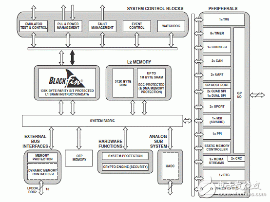
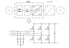
图1. ADSP-BF70x Blackfin处理器系列框图
BLACKFIN+ PROCESSOR CORE
As shown in Figure 1, the processor integrates a Blackfin+ processor core. The core, shown in Figure 2, contains two 16-bit multipliers, one 32-bit multiplier, two 40-bit accumulators (which may be used together as a 72-bit accumulator), two 40- bit ALUs, one 72-bit ALU, four video ALUs, and a 40-bit shifter. The computation units process 8-, 16-, or 32-bit data from the register file. The compute register file contains eight 32-bit registers. When performing compute operations on 16-bit operand data, the register file operates as 16 independent 16-bit registers. All operands for compute operations come from the multiported register file and instruction constant fields. The core can perform two 16-bit by 16-bit multiply-accumu-lates or one 32-bit multiply-accumulate in each cycle. Signed and unsigned formats, rounding, saturation, and complex mul-tiplies are supported. The ALUs perform a traditional set of arithmetic and logical operations on 16-bit or 32-bit data. In addition, many special instructions are included to accelerate various signal processing tasks. These include bit operations such as field extract and pop-ulation count, divide primitives, saturation and rounding, and sign/exponent detection. The set of video instructions include byte alignment and packing operations, 16-bit and 8-bit adds with clipping, 8-bit average operations, and 8-bit subtract/absolute value/accumulate (SAA) operations. Also provided are the compare/select and vector search instructions. For certain instructions, two 16-bit ALU operations can be per-formed simultaneously on register pairs (a 16-bit high half and 16-bit low half of a compute register)。 If a second ALU is used, quad 16-bit operations are possible. The 40-bit shifter can perform shifts and rotates and is used to support normalization, field extract, and field deposit instructions
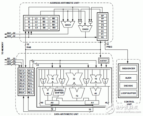
图2. ADSP-BF70x Blackfin+处理器核框图
评估板ADSP-BF707 EZ-KIT Lite
Thank you for purchasing the ADSP-BF707 EZ-KIT Lite®, Analog Devices, Inc. low-cost evaluation system for the ADSP-BF70x Blackfin® processors.
The ADSP-BF707 processor is a member of the Blackfin family of products. Blackfin processors combine a dual-MAC state-of-the-art signal processing engine, the advantages of a clean, orthogonal RISC-like microprocessor instruction set, and single-instruction, multiple-data (SIMD)multimedia capabilities into a single instruction-set architecture. New enhancements to the Blackfin+™ core add 32-bit MAC and 16-bit complex MAC support, cache enhancements, branch prediction and other instruction set improvements—all while maintaining instruction set compatibility to previous Blackfin products.
The EZ-KIT Lite is shipped with all of the necessary hardware—you can start the evaluation immediately. The package contains the standalone evaluation board, CE-approved power supply, and USB cable. The EZ-KIT Lite version ships with an ICE-1000 emulator, while the EZ-Board® version is supported by the ICE-1000 or ICE-2000 emulator.Expansion Interface III is provided for connecting a camera or audio extender board.
Traditional mechanical switches for changing the board’s factory setup have been removed in favor of I2C controlled software switches. The only remaining mechanical switches are the boot mode switch and push buttons.
The evaluation board is designed to be used in conjunction with the CrossCore® Embedded Studio (CCES) development tools to test capabilities of the ADSP-BF707 Blackfin processors. The CCES development environment aids advanced application code development and debug, such as:
Create, compile, assemble, and link application programs written in C++, C, and assembly
Load, run, step, halt, and set breakpoints in application programs
Read and write data and program memory
Read and write core and peripheral registers
评估板ADSP-BF707 EZ-KIT Lite 主要特性:
Analog Devices ADSP-BF707 processor
184-ball BGA package
25 MHz CLKIN core oscillator
DDR2 memory (DMC0) chip
128M x 16-bit (2G bit)
Micron MT47H128M16
Quad SPI Flash (SPI2)
32M bit serial flash memory
Winbond W25Q32
RF Wireless
4 x 2 connector
0.05” socket
Universal Asynchronous Receiver/Transmitter (UART0)
FTDI FT232RQ USB to UART converter
USB Mini B connector
Controller Area Network (CAN) interfaces
CAN0—NXP TJA1041 transceiver and RJ11 connector
CAN1—NXP TJA1041 transceiver and RJ11 connector
USB0 interface
Micro AB connector
HADC
VIN0 RTC battery through jumper
VIN1 timer through RC
VIN2 0.1” header
VIN3 0.1” header
RTC
16MM coin connector
3V 125 mAh Li-ion
CR1632
RESET controller
Analog Devices ADM6315 microprocessor supervisory circuits
Debug (JTAG/SWD/TRACE) interface
JTAG/SWD/SWO 10-pin 0.05” header for use with ADI emulators
TRACE/JTAG/SWD 38-pin Mictor header
Power measurement
INA3221 to measure 3V, VDD_INT and VDD_EXT
INA230 to measure VDD_DMC0
LEDs
Six LEDs: one power (green), one board reset (red), one SYS_FAULT (red), and three general-purpose (amber)
Push buttons
Three push buttons: one reset and two IRQ/Flag
Expansion Interface III connectors (EI3)
SMC0
PPI
SPORT
SPI
UART
TWI
TMR
GPIOs
PWR_IN
GND/3.3V output
External power supply
CE compliant
5V @ 3.6 Amps
Other features
SD/MMC memory connector
Boot mode switch
0.05-ohm resistors for processor current measurement
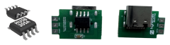
图3. 评估板ADSP-BF707 EZ-KIT Lite外形图
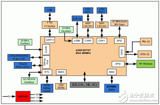
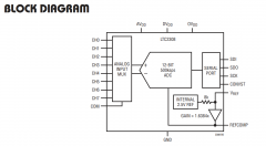
图4. 评估板ADSP-BF707 EZ-KIT Lite框图
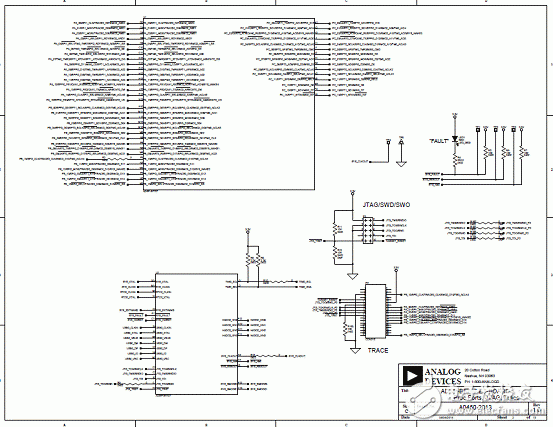
图5. 评估板ADSP-BF707 EZ-KIT Lite电路图(1)
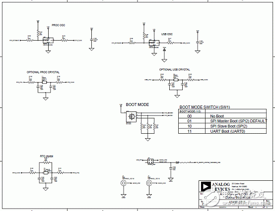
图6. 评估板ADSP-BF707 EZ-KIT Lite电路图(2)
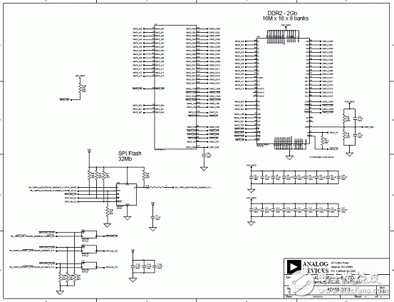
图7. 评估板ADSP-BF707 EZ-KIT Lite电路图(3)
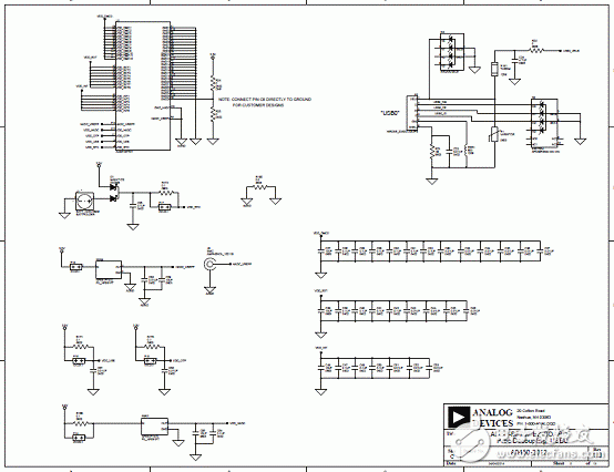
图8. 评估板ADSP-BF707 EZ-KIT Lite电路图(4)
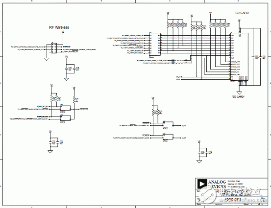
图9. 评估板ADSP-BF707 EZ-KIT Lite电路图(5)
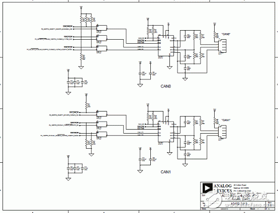
图10. 评估板ADSP-BF707 EZ-KIT Lite电路图(6)
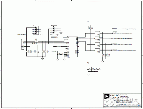
图11. 评估板ADSP-BF707 EZ-KIT Lite电路图(7)
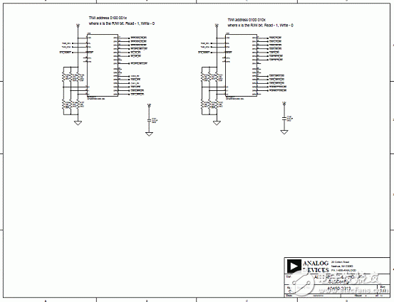
图12. 评估板ADSP-BF707 EZ-KIT Lite电路图(8)
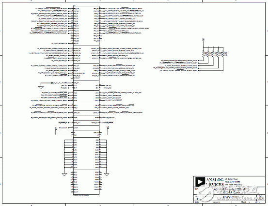
图13. 评估板ADSP-BF707 EZ-KIT Lite电路图(9)
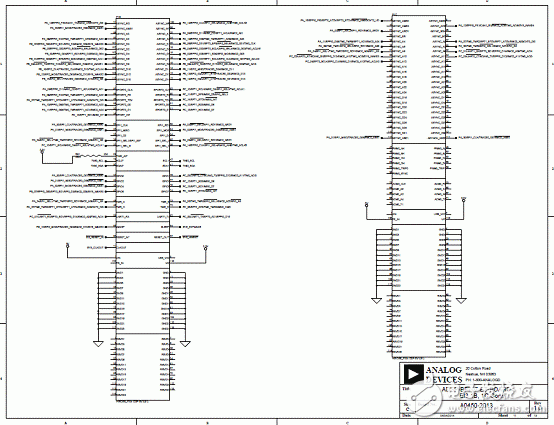
图14. 评估板ADSP-BF707 EZ-KIT Lite电路图(10)
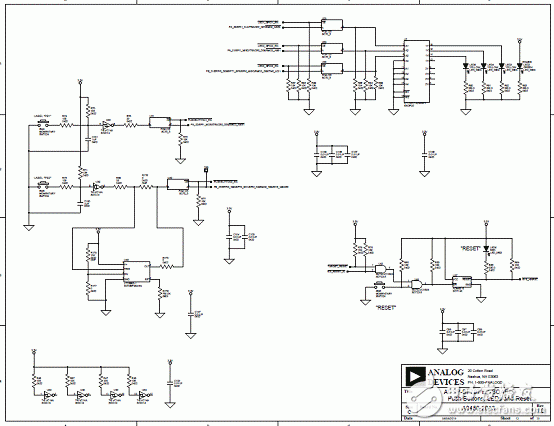
图15. 评估板ADSP-BF707 EZ-KIT Lite电路图(11)
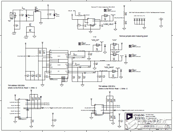
图16. 评估板ADSP-BF707 EZ-KIT Lite电路图(12)
评估板ADSP-BF707 EZ-KIT Lite材料清单:
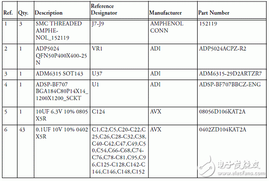
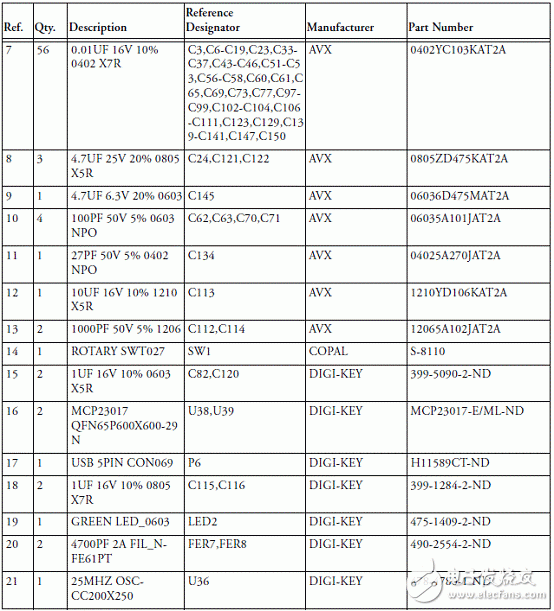
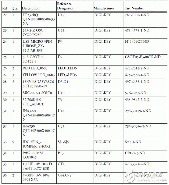
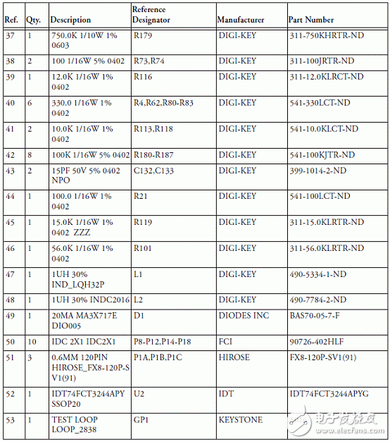
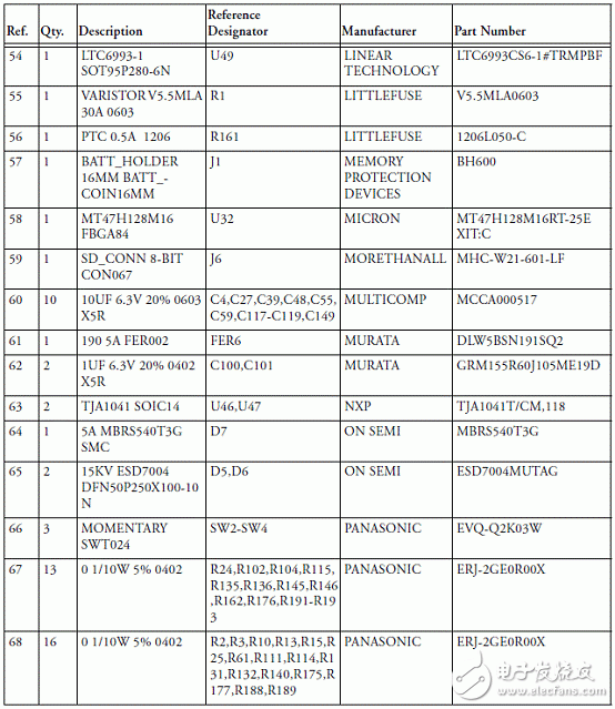
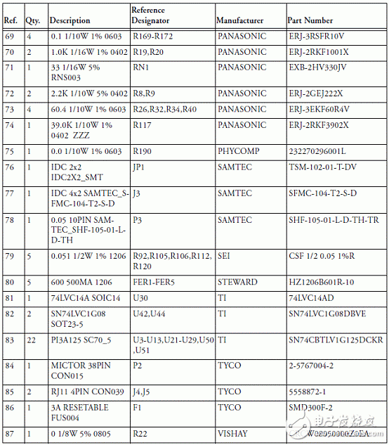
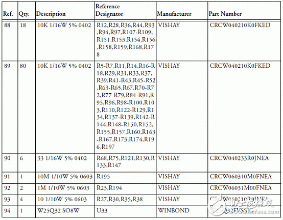
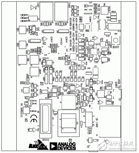
图17. 评估板ADSP-BF707 EZ-KIT Lite PCB元件布局图:顶层
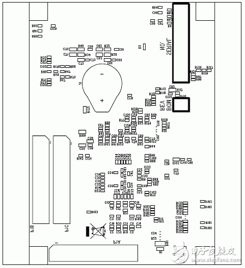
图18. 评估板ADSP-BF707 EZ-KIT Lite PCB元件布局图:底层
更详细的评估板ADSP-BF707 EZ-KIT Lite PCB布局设计图见:
评估板ADSP-BF707 EZ-KIT Lite PCB布局设计图.pdf
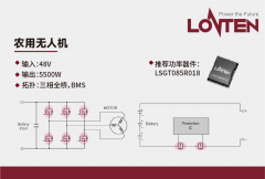
龙腾半导体SGT MOSFET LSGT085R018在智慧农业无

 关注微信
关注微信